BGA Design in 4 layer PCBs: Circuit Routing and Pin Limitations
Apparently, adults enjoy connecting the dots just like children. However, there’s a twist in the adult version of the game: instead of joining dots to draw a T-rex on paper, the adult version involves creating as much square with grids of dots and blocking the opponent from doing so. Or, sometimes adults just like the simple pleasure of creating an isometric design.
Unfortunately, there’s no winner if you’re making boxes from the tiny dots from a BGA pad. In a BGA design, the trick to success is ensuring the ‘dots’ are properly fanned-out on a 4 layer PCB.
Challenges in BGA Design on a 4 Layer PCB
The demand for compact electronics has spurred the development of electronics chips in the BGA form factor. Hundreds of signal and power pins are now littered underneath a smaller IC, compared to its QFP counterpart. It’s great news for marketers who promise tinier consumer products, but the nightmare for PCB designers is about to start.
Most of the BGAs would have a ball pitch between 0.5 mm to 1.0 mm. As the BGA package is usually meant for FPGA and microcontrollers, the number of pins underneath the IC could range between 200s to 2000s. To make matters worse, the diameter of the balls decreases as the pitch gets smaller.
Fanning out the traces on a BGA chip and the manufacturing process is fraught with challenges. For example, a BGA chip with a 1.0 mm pitch and a 0.45 mm landing pad can be routed with a 0.18 mm trace on a channel. A channel in BGA routing means the space between two landing pads on the X or Y-axis.
Typically, squeezing a 0.18 mm trace between two 1.0 mm pitch is not an issue, except that BGA’s pads are arranged in a dense grid pattern. This means you’ll need to figure out how to connect the inner pads to their respective nets. The task gets much more complicated when you have a BGA with half the pitch size.
Fanning out BGA on a 4 Layer PCB can be challenging.
As both traces and clearance gets smaller, issues that trouble PCB designers start creeping up. You’ll be worrying about crosstalk, EMI, and manufacturability. Some manufacturers may not have the capacity to reliability produce narrow traces and close spacing that are used in BGA design.
BGA Pin Limits For A 4 Layer PCB
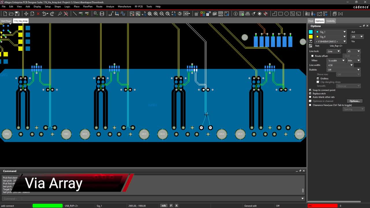
Most BGA strategies start by fanning out the outer first and second rows to the same layer of the chip. Then, the third and fourth rows of pins are routed via the dog-bone style to a different layer of the PCB. Dog-bone routing is making a short connection of the BGA landing pad to a via placed diagonally and in the center of four adjacent pads.
On a 4 layer PCB, the middle layers are usually power planes and ground, which are connected to the supply and ground pins of the BGA chip. This means that all signal layers will have to be fan-out to either top or bottom layers.
The question that begs an answer isn’t how many pins on a BGA chip can be routed on a 4 layer PCB, but rather the number of the rows on the chip. Assuming a single trace is routed on a channel, you can route a 4 rows deep BGA chip on a 4 layer PCB.
BGA routing is highly dependent on the pitch, pad size, and available areas.
Maximizing Routability For BGA on a 4 Layer PCB
PCB designers are an ambitious lot and they will happily take up the challenge of routing a denser BGA chip on a 4 layer PCB. However, this means routing two traces on a channel instead of one. Doing so requires consideration of manufacturability, as well as issues like crosstalk.
You’ll also need to think about the pitch size, ball diameter, and the available routing space before deciding if you can fit a BGA chip with 5 or more rows of pins on a 4 layer PCB.
Whether you’re looking for a solid base of DRCs to work from, or looking for an all around system design, analysis, and verification platform, Cadence assuredly has the tools for you. Setting up fanout constraints on OrCAD PCB Designer and working closely with your manufacturer helps to minimize issues with BGA routing.
If you’re looking to learn more about how Cadence has the solution for you, talk to us and our team of experts.