OrCAD X: Accelerating PCB Design Automation
Key Takeaways
-
Instead of being a clever buzzword for replacing engineers, PCB design automation is an essential aspect of competitive board development.
-
For optimization, design automation should simplify your workflow, minimize or reduce repetition and errors, and maximize collaboration and co-design.
-
OrCAD X provides automated visual integration, in-design DFM, and cloud-based collaboration that allows you to maximize the speed and efficiency for your PCB design workflow.

OrCAD X is raising the bar for PCB design automation
In simple words, electronic design automation (EDA) refers to software tools used to facilitate the process of electronic design. In the not-too-distant past, EDA functionality was basically limited to some degree of autorouting for your layout design. Although a significant asset for engineers and board designers, the need for faster, more accurate PCB design requires increased capability. With the incorporation of advanced technologies, like AI for PCB layout design, OrCAD X is meeting this need for accelerated PCB design automation.
OrCAD X PCB Design Automation Features
|
OrCAD X Feature |
Benefits for PCB Design Automation |
|
Automatic real-time component supply chain data updates |
Improves the speed and efficiency of schematic design. |
|
Automatic in-design DRC compliance analysis |
Significantly reduces the time for PCB verification. |
|
Automatic concurrent design and collaboration |
Real-time simultaneous data access and revision updates enable synchronized (instead of sequential) team collaboration. |
|
Automatic 3D visualization and analysis |
Helps reduce the design time for ECAD/MCAD collaborations. |
Why Is Automation Important For Board Development?
As the market for products that utilize electronics gets more competitive, PCB designers need to optimize their design for manufacturing and assembly (DFMA) and maximize benefits and efficiency. Besides operational concerns, PCB designers are challenged by the need for electronics with smaller, faster components and increasingly less board real estate to work with. This density only elevates potential operational concerns. For example, many board designs, including high-speed design, require that electromagnetic interference (EMI) be minimized, while electromagnetic compatibility (EMC) is maximized to achieve reasonable signal integrity.
To remain competitive, PCB designers need EDA software that is equipped with features and tools that help in mitigating these issues. EDA software has long grown beyond a simple program that enables designers to route the components on the PCB. Today, capabilities that aid in component selection, error-checking, PCB verification, and documentation are needed.
Modern EDA software is also built with simulation and analysis tools that are integrated within both schematic capture and PCB design phases. These tools help PCB designers evaluate component and circuit operation and performance and spot potential issues before the design is finalized and manufactured. Issues like EMI can be significantly reduced when PCB designers have tangible data to work with during the design stage.
OrCAD X Solutions for Automated PCB Design
The OrCAD X platform harnesses the power of Cadence Allegro X and delivers an intuitive, yet comprehensive environment to help PCB designers optimize their workflow. This includes the following capabilities that elevate PCB design automation.
Real-Time Component Supply Chain Data

As shown above, OrCAD X provides inherent real-time supply chain resiliency with Live BOM. With Live BOM, designers and developers can make smart choices about which component to use based on accurate availability and status data.
Interactive Placement and Routing
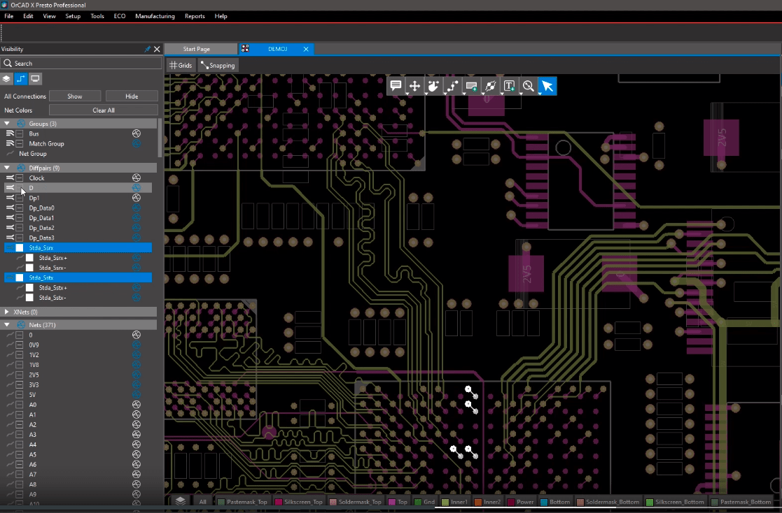
Route highlights of some receiver and transmitter differential pairs in OrCAD X Presto PCB Editor
By far, the most difficult aspects of PCB layout are placing components and routing traces. OrCAD X Presto PCB Editor is designed to minimize the pain of this often tedious and time-consuming process. The platform includes layout tools that put the power to create the workspace in your hands. Interactive routing along with grid and snapping functionality within OrCAD X, allows for precise control over signal paths and optimized signal integrity, reducing design errors through constraints and real-time feedback.
In-Design DRC

Constraint specification for in-design DRC
Constraint specification is mandatory to ensure your design adheres to your CM’s DFMA rules and industry standards. OrCAD X gives you several options for specificity and DRC execution as you design.
Documentation and Collaboration
Another feature of OrCAD X that can significantly reduce design time, especially for teams, is template-driven automated fabrication and assembly documentation generation with Live DOC, shown below.

OrCAD X Live DOC perspective
Live DOC automates design documentation using fabrication and assembly data templates using the always up to date design data from your database.
3D Visualization and Analysis

3D visualization analysis with OrCAD X
The days of siloed electromechanical design and development are rapidly disappearing. Yet, most ECAD and MCAD design tools are incapable of real-time co-design. OrCAD X provides the framework for breaking through this barrier to efficient ECAD/MCAD collaboration.
Optimizing PCB Design Automation
The right EDA software will help you make supply chain-aware component selections, reduce or eliminate common errors, and expedite the PCB development process. By choosing the latest OrCAD X platform, you can maximize PCB design automation to accelerate your innovative process. You also gain integration access to the wide range of industry-leading PCB Design and Analysis Software available from Cadence.
Leading electronics providers rely on Cadence products to optimize power, space, and energy needs for a wide variety of market applications. To learn more about our innovative solutions, talk to our team of experts or subscribe to our YouTube channel.