RF Via Transitions in High-Speed Designs
Key Takeaways
- Via transitions in RF PCB layouts require meticulous design, especially at GHz frequencies.
- For HDI PCBs, proper via transition design and antipad sizing are crucial for maintaining impedance control.
- Ground plane via spacing, grounded coplanar waveguide design, and appropriate use of stitching vias are essential for different frequency bands
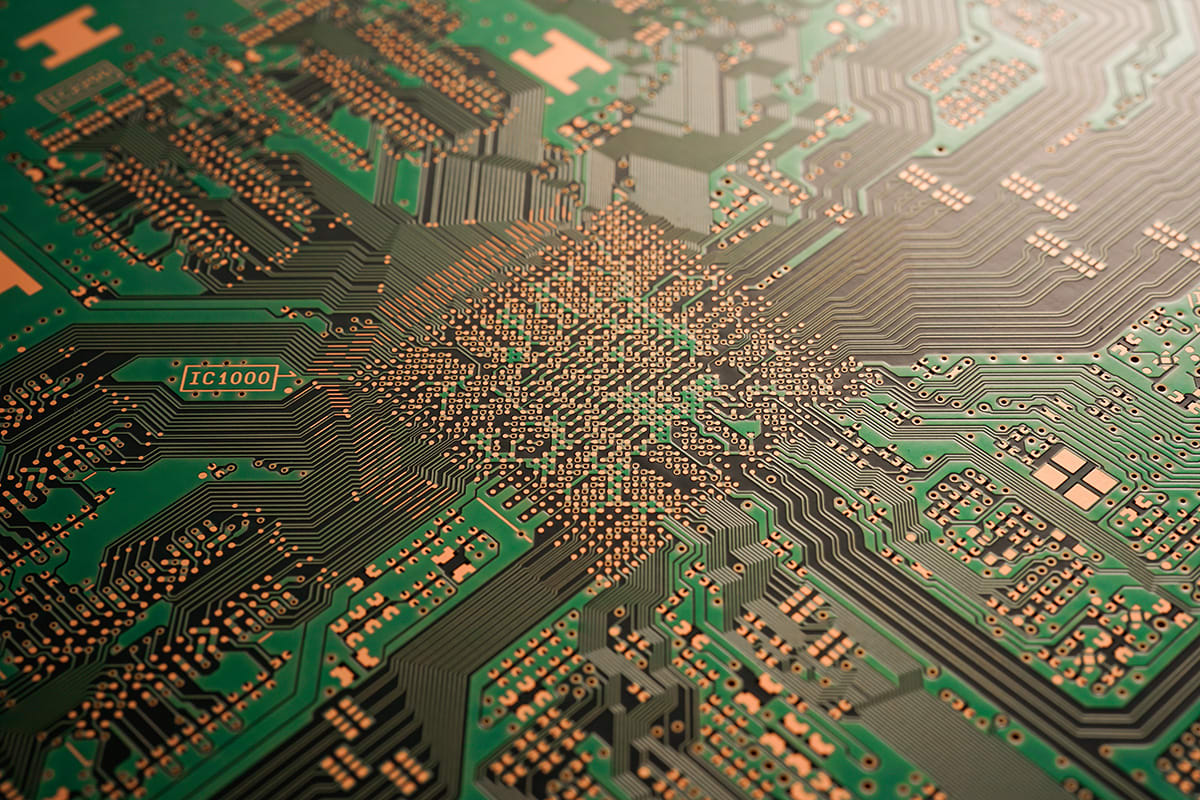
PCB closeup of fanout from a high-speed chip with RF transition vias coming off.
When working with RF and very high-speed digital designs, many engineers focus primarily on controlling the impedance of the traces, often overlooking the significance of RF via transitions. In RF PCB layouts, the use of an RF via transition should be approached with caution. While several factors need consideration when deciding whether to incorporate vias into a PCB layout, the most critical factor is the signal frequency.
When signal bandwidths are very broad, extending into the GHz range of RF, the via transition must be meticulously designed to ensure low return loss at the via's input. Additionally, the placement of the via should not alter the insertion loss of the equivalent channel without the via.
Best Practices for Transitioning Vias Between Layers
|
Best Practice |
Description |
|
Ground Plane |
|
|
Grounded Coplanar Waveguide |
|
|
Slow Signals with rise times significantly over 20 ns |
|
|
Channels less than 3 GHz Bandwidth |
|
|
Channels over 5 GHz Bandwidth |
|
|
Channels greater than 90 GHz Bandwidth |
|
In Choosing High Density
If you are planning to use HDI buildup for your board and require backdrilling consider employing a high-density approach with blind or buried vias for your layer transitions. Even on HDI PCBs with impedance-controlled stack-ups that utilize microvias of limited depth (typically 100um to 150um) and no stubs, improper via transition design could degrade return loss.
Antipads Role in Determining Impedance
Antipads are the spaces between the via plating and the connection to the adjacent copper structure. In high-speed and RF PCB design, via transitions must pass through at least one plane layer, requiring the correct sizing of the antipad in the plane layer to help determine the impedance. By adjusting the antipad dimensions, we can alter the capacitance associated with a via, thereby directly controlling its impedance (discussed further below).
RF Via Transitions in High and Low-Speed Designs
The impact of via transitions on traces must be carefully considered to ensure the overall performance of the PCB design.
Low Frequency Considerations (Below 3 GHz)
At frequencies below 3 GHz, the input impedance of via transitions often strays significantly from 50 Ohms if there is a nearby ground return via. Thus, specific stitching via structures are generally unnecessary unless dealing with very fast channels.
Also at low frequencies, the impedance of vias on an RF transmission line also closely matches the downstream transmission line sections, provided these sections are impedance-matched. This reduces the need to worry about the via's impedance
High Frequency
As frequencies increase, especially at mmWave frequencies, the significance of via impedance grows due to parasitic effects that can impact signal integrity.
Especially with bandwidths above 5 GHz, in the absence of stitching vias, transitions appear inductive. This trend continues as via transitions appear inductive with impedances increasing by factors of 3 to 4 up to 30 GHz or so. At even higher frequencies, the capacitance effects take over resulting in impedance decreasing up until around 50 GHz.
Mitigating High-Frequency Impedance Issues
Implementing stitching vias and reducing the size of the antipad can effectively mitigate the rise in impedance within the 5 to 50 GHz frequency range. This is because the stitching vias and the antipad collectively influence the capacitance in parallel to the signal vias, thereby reducing the overall characteristic impedance of the via.
Moving these elements closer together further decreases the impedance, aligning it more closely with the desired impedance target (either single-ended or differential).
Theory and Solvers
Online via calculators often inaccurately predict constant via impedance across frequencies, failing to reflect its capacitive start and subsequent inductive behavior as frequency increases. These calculators typically overestimate propagation delay, resulting in incorrect phase delay estimates, which is critical for applications like mmWave phased arrays. Even more, standard via calculators do not consider stitching vias, essential for setting precise via transition impedance at high frequencies.
The complexity of accurately determining via impedance for varying layer counts and stitching structures makes the problem analytically intractable. For this reason, engineers frequently rely on 3D EM simulation software to simulate and optimize via transitions, although simpler structures with direct return paths may not require such detailed simulations.
OrCAD X Features for RF Via Transitions
|
Feature |
Description |
|
HDI Design |
|
|
Via Stitching |
|
|
Constraint Manager |
|
|
Design Rule Checks (DRC) |
|
|
Signal Integrity Analysis |
|
When dealing with RF via transitions, ensuring optimal signal integrity and impedance control is paramount. Explore more about how Cadence's PCB Design and Analysis Software can enhance your design process and take advantage of the advanced capabilities of OrCAD X for your next project.
Leading electronics providers rely on Cadence products to optimize power, space, and energy needs for a wide variety of market applications. To learn more about our innovative solutions, talk to our team of experts or subscribe to our YouTube channel.