Printed Circuit Board Design - Implementing Flash Memory
There are different types of memory and one of the distinguishing features is if the memory remembers anything once the system is shut down. Non-volatile memory stays around for the next session while the volatile memory lives up to its name and melts away between uses.
A Little History With Flash Memory Used For Storing Software Rather Than Data
Flash memory is that first kind. Your data is saved for posterity. Back in the old days, the physical manifestation of flash memory was the EEPROM. The acronym expands out to Electrically Erasable Programmable Read-Only Memory. This was typically a 20 pin DIP package that could be plugged into a socket for programming. Some of them could only be flashed one time. Those were known as PROMs.
When I worked in telecom, the memory devices would come in tubes and the registers would be cleared, “all zeros”. The production line had a gang programmer but my lab equipment could only flash one at a time. Of course, it was at a static-safe desk with an ESD strap around my wrist to make sure I didn't fry the devices.
Before I could even start, an Engineer had to come over and check that the programming was up to date for the intended use. Those checkpoints and log books were essential to meeting customer requirements. Those requirements were borne out of previous disasters. We used sticky labels to hand write the dash-number revision of the information that was loaded on each device. We’re talking about the mid to late 1980s here.
Modern Form Factors and Use Cases For Flash Memory
Over the years, the DIP package gave way to surface mount options as well as more portable use-cases. We have SD Card readers that will mount along the edge of the printed circuit board with access to the outside world. This makes it easy to transfer data by plugging into another SD Card reader. You’d normally see about eight signal pins and a number of chassis mounts for mechanical stability.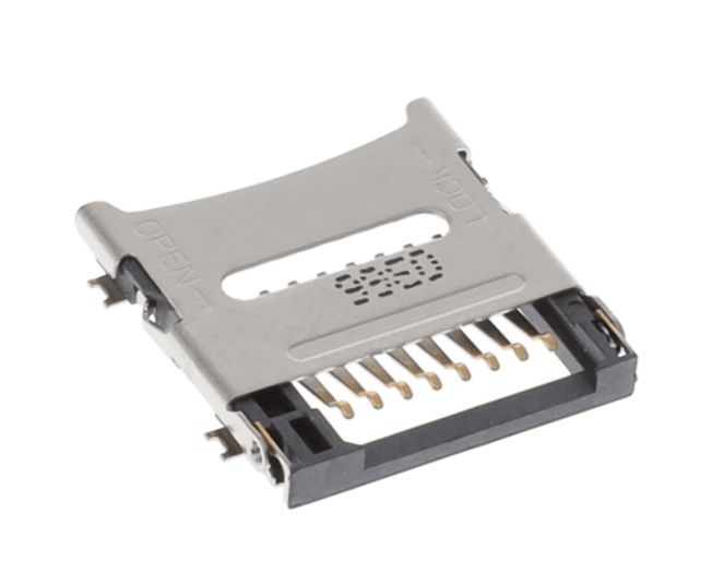
Figure 1. A cage for a micro-SD card showing the contact points. You’re normally routing the signals to a microcontroller or SOC just as you would any kind of memory. Image Credit: Amphenol
Another form factor for external NAND Flash memory is the USB dongle. Chances are unlikely that we’d be tasked with creating the PCB for one of those. The main reason is that there are just so many outfits manufacturing these items. They will put your logo on the outside and call it a day. There are different USB types but they’ll typically use the good old USB-A connector.
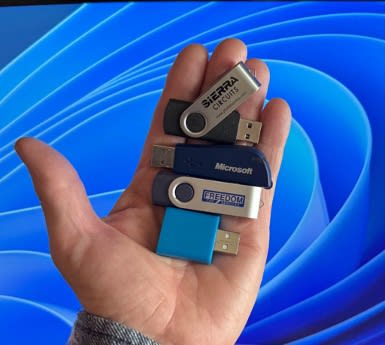
Figure 2. Who doesn’t have a fist full of promotional USB dongles? Image credit: Author
If you are going to create a dongle it will most likely use the USB 3.1 type C connector. It will probably be somewhere between 64 gigs and a terabyte of storage. The multiple superspeed lanes will be useful in transferring that volume of data as a video stream or similar use case. These are not the kind given away at the trade shows.
Solid State Memory Instead of a Disk Drive Using the PCIe Standards
More deeply embedded flash memory is likely to be found on our portable devices in the form of solid state memory in place of the traditional disk drive. Those SATA architectural conventions are still in play while solid state drives typically use some version of the PCIe standards.
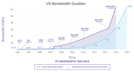
Figure 3. The PCI bus I/O bandwidth roughly doubles over any three-year period. A motherboard would have two connector slots minimum; one for graphics and another for memory. Both would be sensitive to location with respect to the SOC. Image Credit: PCI SIG
The PCIe standard is versatile in terms of swappable lanes and multiple configurations. PCIe has grown along with the computer industry by adding lanes and increasing data rates. The PCIe special interest group supports other types of peripherals as well. Mini Card and Half Mini Card versions of PCIe were used as WiFi cards before Wifi was incorporated into our laptops.
Implementing Flash Memory on a Printed Circuit Board
Incorporating, in this case, refers to bringing the circuit onto the motherboard; also known as a Main Logic Board or MLB. Printed Circuit Board mounted Flash memory comes in various packages including old-school TSOP and the fresher BGA versions. One thing these packages seem to have in common is an abundance of no-connect pins.
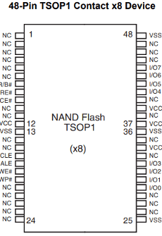
Figure 4. Here’s an example of a surface-mount FLASH memory device. Out of 48 pins, 25 of them are floating. There are 8 I/O pins, a similar number of control lines (collectively known as “Command Interface Logic”) to enable the usual functions and then a few VCC and VSS pins to power the two memory chips that are stacked up inside the package. Image Credit: SkyHigh Memory.
A few years after releasing the 48-pin TSOP package, the 63-pin BGA was added to the lineup. It uses the same two stacked dice for a total of 8Gb of memory. The pin pitch is a generous 0.8 mm which allows normal plated through-hole vias. The silicon is large but that is normal for memory devices.
Why Memory is Normally in a Separate Package
The size of the features for the memory IC fabrication process is enormous compared to the geometry used for the processor gates. There will likely be a memory cache right on the processor but it is kept to a minimum. When it comes to mobile/wearable applications, the RAM is often stacked on top of the SOC so the flash memory is often the only one that concerns us as PCB designers.
That was not the case for the XBOX as that main logic card had more DDR than I had ever seen on one board. I thought that eight was enough. In any case, Microsoft had a way to make sure that I didn’t touch the memory. They had many scripts and one of them turned traces into equivalent shapes which were locked down.
A separate script restored them but we don’t even tread those waters. There are EMI implications to how we route the flash memory. We’re free to improve the circuit until it is etched into copper for the first time. If that iteration works, you’re stuck with it so don’t rush these things.
Extending signal integrity to the control lines as well as the data bus
The command interface logic that I mentioned in Figure 3 isn’t controlled impedance but that doesn’t mean that we can route those traces over voids in the reference planes. Every signal should route within a faraday cage. The main difference is that line width and space constraints will allow denser routing of the non-controlled impedance traces. Our concern isn’t so much about impedance as it is electromagnetic interference within the system as well as outside of the box.
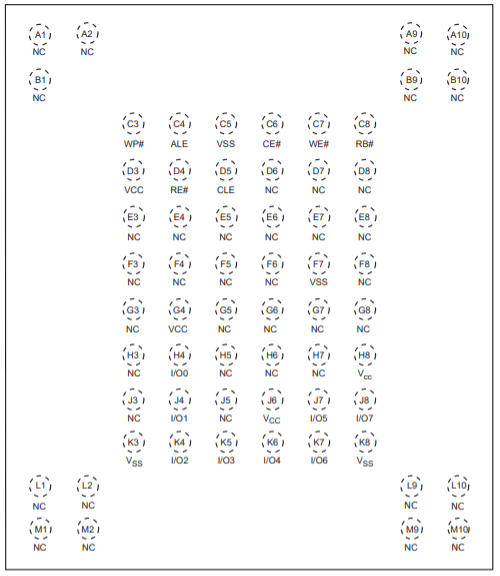
Figure 5. This ball map includes several outlying pins that do nothing more than hold the component in place. The vendor can use an IC with smaller dimensions and omit the outer rows. That reduces the package size down to near the length and width of the 48 central pins. Image Credit: SkyHigh Memory.
Naturally, the particulars of the device will drive the technology. On-board read/write protocols for flash memory include I2C, SPI and EMMC. Each will have its own interrelationships and ensuing design rules. While it may be stated that you have some degree of tolerance in terms of length matching, I find the system engineers want to retain all of the margin they can get.
How Much Length Matching is Enough?
If the memory lines can all be the same length, then there’s no room left to haggle about it. I would prefer to find the longest line and subtract 90% of the available skew and route the clock to that length. The long tentpole would be as long as the clock plus the positive tolerance. The shortest traces are only to be lengthened until they meet the minimum deviation with the same 10% cushion.
The clock is just long enough to solve for the longest line. From there, the short traces are meandered just enough to meet the threshold between too short and just enough compared to the clock. That would be most efficient in terms of effort and overall trace length which should minimize radiation at the cost of using up the available margin.
The other school of thought is to match every line as close as possible. Stretching all of the lines, including the clock. to equal the longest one will leave the maximum margin. In practice, we’re likely to fall somewhere between those two limits. It seems like the fewer lines you have, the more the length matching matters. You should already know how to make the concerned Engineers comfortable. Knowing the specs and the personalities involved will help you do this in a FLASH.