Managing Printed Circuit Board Designers
Being a Manager isn’t for everyone. Beyond technical skills, the boss is responsible for resource allocation and managing risk. In the electronic design arena, the manager is straddling the line between being a technical person and a people-person. Beyond that, the manager of an employee involved with creative electronic endeavors has to understand the uncertainties and ensuing challenges that come with a design project.

Figure 1. A good chair is almost as important as a large screen. The designer incorporates data sheets and app notes with the schematic and the power tree along with email and other micro-communications. This is on top of the actual layout where the more we can see, the more we can do. Image Credit: Author
Of course, the Electrical Engineer will normally say that the schematic is complete on the day that it is supposed to be. Same for the Mechanical Engineer. Ever the optimist, everything is going according to plan - until the day that it isn’t. Surprise! (Not really surprising)
What Makes PCB Design Work Different?
One of the interesting things about being a printed circuit board designer is that no two boards are exactly alike. Every day is something new. That alone makes it hard to quantify the work involved with a new project. There are some aspects that can be seen as repeatable but the details will always vary.
One of the bellwethers for scheduling is the number of pins in a circuit along with the amount of space allocated per pin. Those two figures in combination can be used as a metric for the expected duration of the design cycle as well as a peek at the layer count and other physical geometry. That leaves a variable that is a little more nuanced which is the nature of the devices involved.
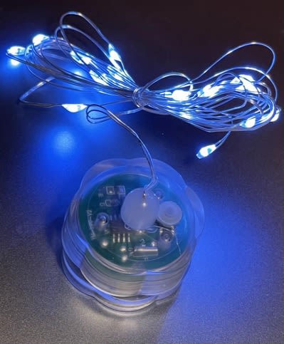
Figure 2. A small printed circuit board can still go sideways if there are factors that are not known to the designer. Image Credit: Author.
Analog signals or high voltage requirements will eat up more real estate than an equal number of digital signals. The exception here is memory, especially DDR devices which will require more space and time for the intensive length matching involved. Any device that is described as a sensor will likely require special handling.
Any of these features are likely to be simulated for signal and/or power integrity. That can mean that it’s not a one-and-done effort but rather an iterative process. When a designer sees something for the very first time, it will very likely take longer to complete. There are usually data sheets and app-notes to digest along with the netlist. I believe that to be one of the reasons that designer job-descriptions are so detailed with specific types of circuit design experience required.
Hiring the Right Designer in the First Place
The company cannot afford to blunder its way through a design program by trial and error. What we see as a result is a great demand for senior PCB designers with specific skill sets. The aspiring applicant needs to be using the institutionalized ECAD software while doing work that has direct parallels to what the hiring manager requires. A start-up will have fewer resources than a multinational enterprise.
That disparity can mean that the start-up will want someone who can pivot over to the test bench and help troubleshoot the boards once it gets to that stage. That requirement will exclude many of the designers who are not as hands-on when it comes to using a soldering iron or a multimeter.

Figure 3. The Kennecott copper mine near Salt Lake City is ¾ of a mile in depth and has been the source for a world record 19 million tons of copper. The PCB industry relies on such efforts. Image Credit: Author.
The hiring manager in a start-up is going to have a harder time finding and recruiting qualified employees. That will be true even if they are not shopping for a designer/technician. Most of the board designers would prefer a company with more perks including job security and even name recognition in many cases. Bigger companies have an advantage in that regard.
The small companies are where individuals can excel without the rigid reporting structure. Like a small town where everybody knows everybody, you can cut through the red tape and get things done. Change the world with your agility. The employees who were there from the early days have the “tribal knowledge” and the chance to grow along with the company. They are usually in a position to include a higher amount of company ownership along with the monetary compensation. Use these advantages as part of the incentive to join the “underdog”.
The Schedule is Most Important but Far From the Only Thing
Stressing schedules over everything leads to shortcuts which can end up backfiring. I had a manager who took it in the other direction. Yes, we needed to finish the work but the overarching goal was to have no questions from the vendor(s) once the design package went out for fabrication and assembly. Give me a four-layer board with no controlled impedance and I can do that.
Once we’re using sequential lamination and specific linewidths for various purposes, the chances of clearing the DFM and DFA cycles without a technical question would evaporate. Even starting with a vendor supplied stack-up and trace geometry was no guarantee that the vendor wouldn’t have a new “and improved” stack-up created to clear out some raw inventory at the shop.
Sending the board out for quotes at multiple fabricators is a sure way to get conflicting DFM reports. Using high density interconnect (HDI) or ultra-HDI is another way to have the vendor try to stall the start-date. I’m not speculating that the vendor does that simply to buy more time. I’ve heard them actually say as much in a moment of candor. I share this so you know how the game is played out on the leading edge.
Design For Manufacturing Defects Come in Different Flavors
One of the tools a vendor has is a method of checking boards that gives three different tiers of technical questions. A red error is something they know that they cannot produce. The orange error flags are there for what can be produced but with a lower potential yield. Eventually, yellow errors would show up for nice-to-have corrections. The first iteration of the board will have to clear out the red errors while letting orange and yellow through. The next rev will be met with DFM flags on the mid-tier orange defects.
Finally, an inexhaustible supply of minor details that could be improved will be reported as time goes by. The vendor isn’t about to disclose this stuff up front. Just know that what was acceptable in the first iteration may only be the tip of the iceberg in terms of what else could be said about any design. Steady incremental improvements seem to be the norm in PCB fabrication.
The End Game
Understanding these outside influences that factor into a PCB design will give the manager a better feel for the uncertainty involved with every project. There are business reasons to expect design execution to include “good enough” work done within the available time frame.
What’s good enough will be a function of the environment where the product will be used. My little Cubesat program had zero tolerance for missing the tape-out date. The rocket was going to go up during the launch window with or without our satellite. Obviously, we couldn’t tolerate any critical failures while in low earth orbit. Knowing this, my manager made sure that we had time to review all of the information going in and coming out of the board design process. It was ok to obsess over details in that case.
Trust But Verify
I came to realize that it’s better to maintain a tight feedback loop with 80% of our time doing work and 20% ensuring that the requirements are being met. With lower stakes, we could reduce the review time to 10%. The ratio will likely fall somewhere between those two values depending on the circumstances.
There tends to be more interest from others towards the end of the cycle. The designer can still get their 90% heads down time. You don’t want to leave them on an island until the final day. Check up on them early and often. Ask what percentage of the job remains to be done in their estimation. Staying abreast of the progress not only shows that you care but also that you want them to succeed.
Figure 4. The portable and plantable tree is powered by the little drum with its string of lights. Just a reminder that a little time off can be a good thing at the end of a strong effort to close the books on a project. A comp day is nice but even an afternoon to decompress shows the spirit. Image Credit: Author.
The typical flow goes from importing the outline to floorplanning and placement on to fan-out and routing including provisions for testing. Bigger jobs should be broken down into segments with milestones to hit along the way. This gives us more visibility into the progress of the overall design effort. Complex designs should not be interrupted as there is so much to keep in mind during the layout.
Visit your designers. Ask if anything is blocking them. Facilitate when necessary. Have a PCB Design service bureau on speed-dial for when a project schedule is at risk. Ideally, they can work the night shift so that the board is progressing around the clock. The design could also be partitioned for parallel work in different areas. That feature can have a bit of a learning curve and requires more coordination than passing the job back and forth.
The designer’s success or failure is partly up to you. Management by walking around is one of the methods that I’ve seen work in practice. You need to keep your finger on the pulse so that corrective action is always on the table. Knowing that I’m making a difference is all the motivation I need. I’m probably not the only one.