Guide to Getting Started with OrCAD X Presto
Key Takeaways
-
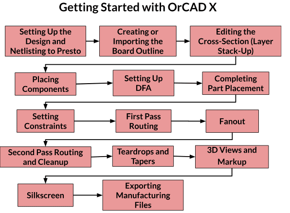
Get started in OrCAD X with setting up the design, netlisting to Presto, importing or creating a board outline, editing the layer stack-up, and placing components according to the design constraints.
-
Routing then begins with a focus on first-pass routing, fanout, and refinement through second-pass routing, teardrops, and tapers, ensuring signal integrity and manufacturability.
-
The design is polished with silkscreen adjustments, 3D views, and markup before exporting manufacturing files.
Comprehensive Guide for Getting Started with OrCAD X
OrCAD X is an incredibly powerful program that enables users to handle every aspect of PCB design, from schematic creation to simulation and layout. In this "Getting Started with OrCAD X" guide, we’ll focus on how to use OrCAD X Presto, covering the basics from beginning to end. This guide will give you the knowledge to confidently navigate the software and make your designs manufacturer-ready. Here’s what we'll cover:
|
Section Title |
Content Covered |
|
Setting Up the Design and Netlisting to Presto |
Launching OrCAD X Presto from Capture, configuring netlist settings, verifying schematic data in Presto, reference designator updates, cross-probing between schematic and layout. |
|
Creating or Importing the Board Outline |
Drawing the board outline manually, importing outline geometry from DXF files, setting keep-in areas, adjusting the design origin. |
|
Editing the Cross-Section (Layer Stack-Up) |
Defining layer stack-up in Cross-Section Editor, adding/removing layers, setting conductor vs. plane layers, thickness, materials, and optionally importing cross-section technology files. |
|
Getting Started with Placing Components in OrCAD X |
How to place components on a PCB in OrCAD X using tools like the Move and Place commands. It covers methods for clustering related parts and leveraging schematic cross-probing for efficient placement. |
|
Setting Up DFA (Design for Assembly) Rules |
Learn to enforce assembly spacing requirements using DFA rules — classifying components by type, defining spacing constraints, and using visual aids like bumpers to avoid errors. |
|
Completing Part Placement |
Focuses on arranging components effectively, starting with larger parts and using tools like rats’ nest visibility and alignment guides. Includes tips for grouping, refining placements, and checking 3D clearances. |
|
Basic Constraints Setup |
Introduces setting up physical and spacing constraints for routing. It guides users on creating and applying “Constraint Sets” for consistent trace widths and spacing while resolving DRC conflicts. |
|
Fanout |
Automating pin fanouts (especially for BGAs or dense devices), applying radial vs. linear fanout modes, assigning fanout direction, controlling via spacing, and adding ground stubs on capacitors. |
|
Second Pass Routing and Cleanup |
Using Slide (hug/shove) to fix DRC spacing or collisions, refining trace paths, editing shapes, stitching vias, aligning route channels, verifying design rules, and making final adjustments. |
|
Teardrops and Tapers |
Explaining the benefits of teardrops at via/pad junctions, adding teardrops to strengthen narrow trace entry points, employing the missing tapers report, adjusting geometry for enhanced manufacturability. |
|
3D Views and Markup |
Switching to 3D display mode, adjusting solder mask/dielectric transparency, viewing internal layers, toggling component visibility, adding comments and markups for design reviews. |
|
Silkscreen |
Placing and moving reference designators, editing text/line shapes on silkscreen layers, embedding pin 1 indicators in footprints, adding board labels/logos, aligning and rotating text to avoid pad interference. |
|
Exporting Manufacturing Files |
Creating Gerbers, NC drill files, and IPC-2581 outputs, reviewing layer setup, generating BOM/assembly drawings via LiveDoc, producing PDFs or step models for mechanical review, assembling all outputs into a manufacturing archive. |
Setting Up the Design and Netlisting in OrCAD X Presto
After finalizing your schematic in OrCAD X Capture, transfer the design data into OrCAD X Presto for PCB layout. In the OrCAD X Capture toolbar, navigate to PCB → Design Sync Setup. Ensure that your Layout Tool is set to OrCAD X Presto rather than the older PCB Editor. This ensures the netlist generation will automatically open your board in Presto.
Next, go to PCB → New Layout. Here, you can specify the name of your PCB file and optionally the subfolder where your new board data will live. If you have no existing board file, leave the “Input Board File” field empty. Upon confirmation, OrCAD X Presto will launch, presenting you with an empty canvas but populated with a list of unplaced components and the nets from your schematic.
Verifying the Netlist and Cross-Probing
In the Properties panel of Presto, you will see a Status section for unplaced components. Clicking the associated link brings up the Search window, listing every component from the schematic. Cross-probing between Capture and Presto is simple:
-
From schematic to PCB: Select a component (e.g., U1) in Capture, and it highlights in Presto.
-
From PCB to schematic: Right-click any component or net in Presto, select Cross Probe, and Capture will locate that same item in the schematic.
This cross-probing ensures you always stay synchronized. If you change a reference designator in Capture, you can update Presto via PCB → Update Layout in Capture, or conversely update from Presto back to Capture with ECO → Update PCB.
Creating or Importing the Board Outline
A crucial step is defining your board boundary. In Presto, go to ECO → Draw Design Outline. You can draw simple shapes such as rectangles, circles, and polygons that can besnapped to a visible grid. Toggle grid visibility and snapping under the Grids or Snapping drop-downs to facilitate precise drawing.
Once drawn, the design outline can serve as your official board boundary, automatically generating keep-in layers (e.g., conductor keep-in and component keep-in) as offset outlines. If desired, you can also set the design origin to a specific point on this new shape.
Importing a DXF Outline
For more complex outlines, you may import a DXF file (commonly provided by a mechanical engineer). Select ECO → DXF Import, point to your DXF file, and confirm the measurement units.
-
The Edit/View Layers step maps your DXF layers (e.g., layer 0) to Presto’s Board Geometry → Design Outline.
-
Once the import completes, your complex board shape appears in Presto. You can again use the Properties panel to define keep-in distances or to change the design origin.
Editing the Cross-Section (Layer Stack-Up)
The next major step in getting started with OrCAD X is to define how many layers your board will have. Whether it’s a 2-layer design or a 16-layer design with inner planes, go to Tools → Cross-Section. In the resulting window, you can add or remove layers and specify their types (e.g., conductor vs. plane). You can also set thicknesses, materials, and other high-speed parameters like dielectric constants if impedance control is required.
Importing a Cross-Section Tech File
If your company or project has a standard layer stack-up, you can import it as a .tcfx file through Import → Cross-Section Technology File. Once imported, your layer structure, thicknesses, and naming conventions are immediately reflected. You’ll see those new layers in Presto’s Visibility panel as well.
Getting Started with Placing Components in OrCAD X
With your board outline and stack-up ready, it’s time to place components. Presto’s Move command typically toggles to a Place command with a right-click selection. You can either:
-
Type reference designators (e.g., R1-R10) to bring up those components on your cursor.
-
Highlight components in the Search window (e.g., selecting all unplaced components) and place them en masse.
-
Cross-probe groups of components from the schematic.
Clustering Related Components
A common practice is to pick functional blocks from the schematic (e.g., a voltage regulator plus its decoupling capacitors) and place them on the board together.
Entering the Placement Command
-
Right-click on the Move command icon to reveal the radial menu and select Place.
-
A helper window titled Place appears with options for series or cluster mode, letting you place components in designated orders or grouped sets.
-
Pressing the X hotkey can toggle the helper window under your cursor for easy access.
Multi-Part Placement
-
You may type a range of reference designators in the text field (e.g., D1-D3) to place them simultaneously.
-
Using commas (e.g., C28, C23, C15) allows sequential placement in reference designator order.
-
From the Search pane, highlight multiple “unplaced” components, then click to place them en masse onto the board outline.
Schematic Cross-Probing
-
In OrCAD X Capture, set a selection filter (e.g., parts only) and box-select a functional block (e.g., a regulator plus its capacitors).
-
Return to OrCAD X Presto, and you’ll see those items highlighted; you can then cluster-place them together for coherent layout.
Visibility and Color Settings
-
Under Visibility, you can reassign unique colors to copper layers, solder mask, or silkscreen by right-clicking All and choosing Rainbow Down.
-
Turn on or off certain geometry groups (e.g., Component Keepin) to reduce clutter.
-
Enabling the assembly Quick View ensures that each placed part shows its reference designator in white text, simplifying identification.
Alignment Tools and Rotations
-
Presto’s alignment guides can auto-snap your placements so reference designators or edges line up neatly.
-
Additionally, you can rotate parts with the R hotkey, flip them to the bottom layer with M, and rely on the Properties panel to set exact rotations or side-of-board settings.
Setting Up DFA (Design for Assembly) Rules
This optional step refines assembly spacing checks in Presto. Certain manufacturers enforce minimum distances between component bodies to facilitate automated pick-and-place or hand assembly. We’ll use Constraint Manager to create a DFA constraint set and classify footprints, ensuring the tool flags any violations of those spacing rules via bumpers and DRC markers.
Accessing DFA in Constraint Manager
-
Select Tools → Constraint Manager and within the worksheet look under Manufacturing → Design for Assembly → Package to Package Spacing.
-
Create a new constraint set with the blue + icon. Right-click to toggle Analysis Mode on or off.
Classifying Components
-
Instead of setting spacing for each footprint individually, group them into classes (e.g., “Chip,” “IC,” “CONNPTH”).
-
Move each relevant symbol into the corresponding class: 0603 capacitors into “Chip,” SOT-23 or QFN parts into “IC,” and connectors/plated-through-hole devices into “CONNPTH.”
Assigning Spacing Rules
-
Specify side-to-side, end-to-end, and other positional spacings (e.g., 0.75 mm for chip parts, 1.25 mm for connectors).
-
Apply the new DFA constraint set to the Top and Bottom assembly layers in your design under the Design folder.
Verifying Spacing with Bumpers
-
With DFA turned on, moving a part close to another displays “bumpers” (small circles) showing minimum allowable distances.
-
These help avoid DRCs by snapping or halting the placement if the required clearance is not met.
-
Visibility of these “DFA bounds” can be toggled in the Visibility panel, letting you see exactly where the tool measures body edges.
Completing Part Placement
Typically, you’ll start with large components (e.g., connectors, main ICs) and then arrange supporting components—like bypass capacitors or interface circuitry—near their associated pins. During placement, you can toggle rats’ nest visibility and alignment guides, re-check spacing constraints, and preview a 3D view of your partially placed design.
Placing Large Components and ICs
-
Turn off object snapping and alignment guides if you prefer free-form movement.
-
Drag and rotate key parts (using hotkey R) until they rest comfortably within the board outline.
-
If a connector or port purposely hangs over an edge, you may see a keep-in DRC that can be waived if it’s intentional.
Managing Ratsnest Visibility
-
Connections can clutter the screen during part placement.
-
Under the Nets section in Visibility, hide power or ground nets to reduce unnecessary lines.
-
Bring them back as needed to see overall part-to-part relationships.
Grouping Functional Blocks
-
In Capture, highlight a module’s components and cross-probe to OrCAD X Presto.
-
Use Place in “Series” mode to drop them one by one around the main device, or “Cluster” mode to keep them grouped.
-
Tweak final positions with the Move command, verifying any minimal spacing or assembly constraints.
Quick 3D Check
-
Enable 3D view in the Visibility → Display panel to confirm part heights and potential interference.
-
Switch back to 2D to continue refining if you spot cramped areas or potential collisions.
Basic Constraints Setup
With parts placed, the next step is establishing foundational constraints for routing. We’ll use Constraint Manager to set minimum and maximum trace widths, neck widths, and spacing rules for power vs. signal nets.
Using The OrCAD X Constraint Manager
The Constraint Manager is your central hub for specifying physical and spacing constraints. Go to Tools → Constraint Manager. On the left, you’ll see categories like Electrical, Physical, Spacing, and more. Typically, you’ll focus on:
-
Physical: Setting min/max trace width, via types, and neck widths.
-
Spacing: Setting gap requirements between lines, pins, vias, shapes, etc.
Defining CSet (Constraint Sets)
Rather than manually populating every net with line widths or spacing values, create “Constraint Sets” for common categories like Signal or Power.
-
For instance, a power net might require a 0.5 mm minimum trace width, while signals get 0.15 mm.
-
In the Physical CSet folder, right-click to Create a new set called “Power” or “Signal,” then assign the relevant widths, neck widths, and allowed via types.
-
Once created, apply these sets to the corresponding nets in the Net folder. The same principle applies in the Spacing domain (for example, 0.15 mm for signals, 0.25 mm for power).
Resolving DRC Conflicts
-
After assigning constraints, refresh DRC checks in OrCAD X Presto.
-
Address any errors like pin-to-pin spacing violations by adjusting spacing or neck widths.
-
The final outcome is a well-defined set of physical/spacing rules that pave the way for clean, consistent routing.
Getting Started with OrCAD X: First Pass Routing
Routing is done primarily via the Add Connect command (default hotkey is F3). Manual mode allows you to ignore other geometry (though you’ll see DRC markers if you violate spacing), while assisted or “hug and shove” mode attempts to avoid collisions by automatically pushing existing traces or hugging around them.
-
Left-click to place segments.
-
Backspace to remove the last vertex.
-
R toggles rotation (if picking up a component mid-route).
-
V drops a via and prompts layer switching.
Working Layer Mode and Multi-Pin Routing
When you drop a via in working layer mode, you’re given a list of valid routing layers to continue on. Switching between top and bottom is a straightforward matter of placing a via and choosing the next layer.
You can also route multiple pins simultaneously by box-selecting them; the tool will auto-generate parallel traces that line up neatly, which is especially handy for bus or memory interfaces.
Ground Plane Shapes
If your design uses planes (e.g., ground on layers 2 and 3), you can quickly stub out ground pins or shape them so they automatically connect.
Placing a shape on a plane layer with net set to GND can instantly resolve multiple unrouted ground connections. The shape automatically expands around pads and other objects per your constraint rules.
Getting Started with OrCAD X in Using Fanout
While manual routing works well for smaller devices, large BGAs or pin-dense ICs often need “fanout” of pins. The Fanout command, found under the same toolbar as Add Connect, can auto-drop small stubs and vias for each pin in a matter of clicks. You can select entire components or just certain pins, and specify radial or linear fanout styles (e.g., outwards, inwards, or both). This feature is particularly valuable for complex packages or large groups of identical pins (e.g., decoupling capacitors that each need a ground via near the pad).
Second Pass Routing and Cleanup
Once your initial routing is in place, you may see DRC errors where lines or vias are too close. The Slide command (default hotkey is S) in assisted mode helps rectify these by hugging or shoving geometry out of the way. In manual mode, it simply moves your trace as you drag it, but will issue DRC warnings if spacing is violated.
Leveraging the Properties Panel and Search
You can quickly modify trace widths across multiple segments by using the Search panel. You can filter for trace widths, select them, and then edit the width in the Properties panel. This approach instantly updates all targeted segments in one shot, which is far easier than individual edits.
Additional Shapes and Stitching Vias
You may want to add copper shapes for improved current flow or heat dissipation under certain components (e.g., a linear regulator or switch-mode power supply). Shapes can overlap, and you can control which has priority in the Shape properties. For heat or EMI considerations, you can pepper your shapes with stitching vias—either by copying a single via multiple times or using the Via Array command with a specified grid spacing.
Getting Started with Teardrops and Tapers in OrCAD X
In getting started with OrCAD X, you want to ensure you’re making your board as reliable as possible. Manufacturing reliability can improve with teardrops at via or pad junctions, especially if there’s a sudden change in line width. Teardrops reduce stress points that might result in open circuits. You can add them with Teardrops/Tapers under the same toolbar as Fanout.
Missing Tapers Report
A built-in Reports feature identifies places where a taper or teardrop might be missing, particularly if the geometry changes from a wide to narrow trace. Once the report identifies these spots, you can selectively apply tapers or manually tweak the line segments until the geometry is correct.
3D Views and Markup in OrCAD X
Switching from 2D to 3D is as simple as going to the Visibility panel’s Display tab and clicking 3D. You can rotate, pan, and zoom your board in real-time. Adjusting the solder mask, conductor, or dielectric opacity reveals internal copper planes or via structures. If you have 3D step models for your components, you can see accurate representations in the 3D view.
How to Do Markup and Comments
For design reviews, you can insert “comments” directly on the board. Draw a rectangle around a suspect area (say, a trace running through a keep-out region), and add a textual note. This comment, along with a snapshot, is saved in the design. Colleagues can reply, marking it resolved once addressed.
Getting Started with OrCAD X Silkscreens
To ensure clear assembly instructions, ensure you have Reference Designator Placements on your silkscreen layers. Using the Move command and filtering for Text, you can drag reference designators to avoid overlapping pads or other text. Each component’s reference designator typically has a “leader line” connecting it to that component. Rotate or mirror them as needed. If you want more robust reference designator shapes (with a user-specified line width), you can customize these in your footprints or globally in your library settings.
Adding Graphics and Custom Notes
Use Add Line or Add Shape with the layer set to Silkscreen Top if you want logos, outlines, or pin 1 indicators on the board’s surface. You can also add textual notes or disclaimers with Add Text on the silkscreen layer. If a certain marking needs to be part of the footprint (e.g., a pin 1 marker for an IC), you can use Edit Footprint to embed that silkscreen geometry permanently into the part’s library definition.
Exporting Manufacturing Files with OrCAD X Presto
How to Generate Gerbers and NC Drills
Under Manufacturing → Export to Manufacturing, you can produce a variety of outputs:
-
Gerber (Artwork): Standard 2D vector files for each copper and non-copper layer (e.g., top, bottom, internal planes, silkscreen, solder mask).
-
NC Drill: Drill files specifying hole locations and tool sizes.
-
IPC-2581: A more modern, single-file standard representing the entire PCB.
-
BOM & Assembly Drawings: You can optionally add a Bill of Materials listing easily with OrCAD X Live BOM.
Presto’s default settings typically suffice—layers, zero suppression, and scaling are auto-configured for standard manufacturing. Once generated, you’ll see .art (or .ger) files for each conductor and mechanical layer, along with .drl for drills and possibly a .rep for a BOM report. Pack them into a single ZIP archive for your manufacturer.
LiveDoc for Assembly Drawings
Beyond raw layer outputs, you can generate assembly or fabrication documents using LiveDoc. Within Manufacturing → LiveDoc, you’ll find a built-in document editor that can place board views, stack-up tables, dimension lines, and notes on one or more pages. Any update to the main PCB is automatically reflected in LiveDoc views. This dynamic documentation helps keep reference drawings in sync with your actual design.
3D Export in OrCAD X
If mechanical engineers need 3D data for enclosure design, you can export a STEP or PDF 3D model under File → 3D Export. Settings include units, hole processing, and whether to show details like plated vs. unplated holes or keep-out regions. Large boards with dense via arrays can yield large STEP files, so be mindful when sharing with team members.
With your final set of Gerbers (or IPC-2581), a BOM, and dimensioned assembly drawings, you’re ready to have your board fabricated and assembled.
As your designs grow in complexity, you can further leverage specialized features, such as differential pair routing, advanced plane-shape editing, blind/buried vias, or high-speed constraints. Until then, you’ve officially gotten the basics of getting started with OrCAD X! Visit the Cadence PCB Design and Analysis Software page to explore how OrCAD X simplifies complex PCB design processes.
Leading electronics providers rely on Cadence products to optimize power, space, and energy needs for a wide variety of market applications. To learn more about our innovative solutions, talk to our team of experts or subscribe to our YouTube channel.