PCB Fabrication With Laser Direct Imaging
Precision is the Name of the Game
When normal chemical etch processes cannot satisfy the requirements, we turn to the light.
Laser Direct Imaging (LDI) is a cornerstone of high precision PCB fabrication. Adoption is on-going so it costs more than traditional fabrication. Nobody wants to overspend on their Printed Circuit Board.
One way to overspend is to find yourself scrapping boards because their construction didn’t meet the stated performance objectives. Saving pennies up front and losing dollars down the road has probably sunk a few enterprises. With the 5G rollout already happening, PCBs are becoming more precise in order to land in the acceptable zone.
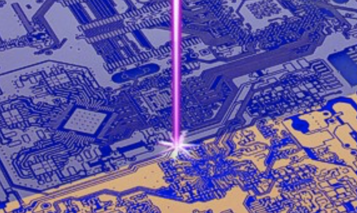
Image Credit: Andus.de - A beam of coherent light can form a circuit and so much more
High Density Interconnect (HDI) is the name of the game. It is getting harder and harder to find all of the necessary chips in packages that support Plated Through Hole (PTH) design. Larger packages are not going to support the rip-roaring data rates we’ll find on the near horizon. The chip houses will continue to shrink the packages leaving the board designer to complete the fan-out.
Why Shrink the PCB and the Components?
The device vendors do not work in a vacuum. Competition from every corner scratches away at the margins. Faster, smaller, more power efficient components are required just to have a seat at the table. Specification wars have the companies racing to produce low power and smaller devices to get their results. It’s all about those numbers and squiggly lines on graph after graph of the data sheets. That one-upmanship between companies continues to drive demand for even more performance at the PCB end of the equation.
The technology roadmaps that the PCB fabrication vendors publish tell the story. Minimum line widths are often given in microns now that one one mil is too coarse of a unit of measure. Traces and spaces are commonly held below 76 um (three mils) on outer layers and 50 (two mils) for inner layers. We have to consider that the layer to layer misregistration has a bearing on making that geometry possible.
With LDI, the metal can be ablated leaving a more rectangular cross section vs. the trapezoid of chemical etching. Cleaner edges are not just for aesthetics. High speed signal propagation improves with cleaner lines. The leading edge of the pulse moves along the outer area of the trace cross-section. This “skin effect” is in play on gigabit data streams.
Laser Defined Soldermask
When the pin to pin pitch falls below 0.4 mm, the typical screen printing application of soldermask comes up short. Lasers leverage the raw artwork data while a slikscreen depends on lining up each PCB panel on a fixture in a separate process. The mechanical nature of the screening process has more variability. In practical terms, it means that the soldermask opening has to be expanded or contracted by a greater amount than would be required using Laser Direct Imaging. We always want the same minimum width for the soldermask dam.
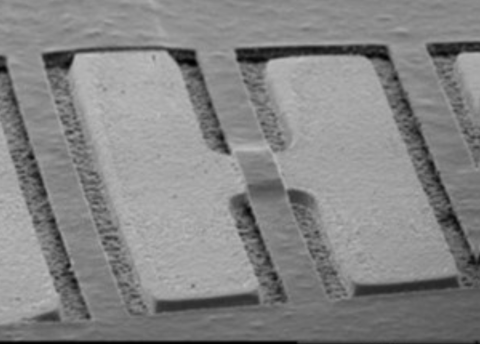
Image Credit: Infotech - Registration is much more precise without using mylar film as an intermediate step
IPC specs call for 100 microns of soldermask. Anything less is considered a sliver. Soldermask slivers have the potential to flake off of the board and do not provide a sufficient solder dam between pads. The 100 micron figure also applies to the difference between the pad size and the mask opening. It is this value that can be narrowed down using LDI.
Molded Interconnect Devices
Merging the circuit board and the housing is one of the promises of additive manufacturing aka 3-D printing. The additive technology is much newer and is geared for one-off pieces or smaller quantities compared to injection molded plastic. The two processes are quite different but the end result is similar. It is possible to metalize a molded plastic piece and then ablate that metal with a laser or leave the whole thing plated as an EMI shield.

Image Credit: Lee Teschler, Design World - Antennas and simple circuits can live on a 3 dimensional surface with no PCB in sight
Capacitive touch points can replace mechanical switches. Shields can conform to the molded chassis. This is something I wished for when I was working on phone chips for Qualcomm. Shields took up a lot of space and wanted to be rectangular. Molded Interconnect Devices can be more organic in shape though there are some limitations as to how the laser can aim the beam. Lee Teschler’s January 2018 article expressed the limits quite well so I’ll share that here.
“One potential problem is that materials can change consistency when they go through a molding process. The changing parameters can affect the electrical qualities of conductors deposited on top. And putting conductors on mechanical components that bend in complicated geometries can change electrical qualities in ways that may be hard to anticipate. Consequently, the mechanical make-up of molded interconnected parts may be sophisticated, but the electronics sitting on the part tends to be relatively simple.”
Wearables and other small form factors would benefit from this technology. It would be tantamount to bonding a flex circuit to a contoured surface. Three layer molded interconnect devices are doable. I was pretty stoked to couch-surf my way to this technology while looking for alternatives to flex circuits.
Image Credit: Multiple Dimensions AG - a Smoke detector with no PCB required
High Precision Edges Using Lasers
The route keep-in is one of the parameters that continues to shrink along with line width. I walked around PCB West last year and asked every PCB fabrication exhibitor on the trade show floor how close could the routing get to the edge. What was once 0.5 mm can be half of that and down to 0.127 mm at several shops though 0.20 mm is the common figure. Below that 0.2 mm threshold, we get into laser cutting the outline.
The caveat with laser-forming the PCB outline is that it can leave carbon deposits along the edge. Another issue is the maximum thickness is generally 0.40 mm or less. With those stipulations in mind, some very intricate shapes can be realized. If you can imagine a 2-D shape, a laser can cut it.
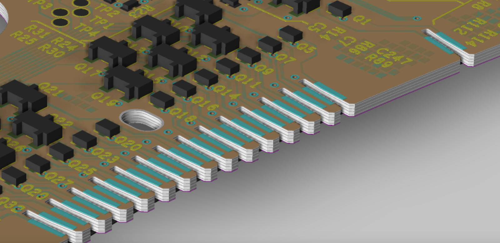
Image Credit: Author - These slots are unobtainable with a mechanically generated board outline; lasers for the win
While lasers drive data around the server farm and drive autonomous tractors around the potato farm, they also step in when we need a helping hand with fabricating our PCBs. This was an outline of some of the ways we benefit from light amplification by stimulated emission of radiation. From Blu Rays to barcodes, lasers enable a wide variety of technology, ours included.