Key Takeaways
-
Emphasize the importance of grid alignment, Design Rule Check (DRC) configuration, and schematic readability, ensuring that schematics are logically arranged from inputs on the left to outputs on the right.
-
Highlight the need for explicit internal terminations, consistent marking of active-high and active-low signals, and the avoidance of text and symbol overlap.
-
Ensure power integrity regulation and good grounding practices. Reliability checks include assessing voltage impacts, calculating power dissipation, and verifying schematic design through design rules checks (DRC).
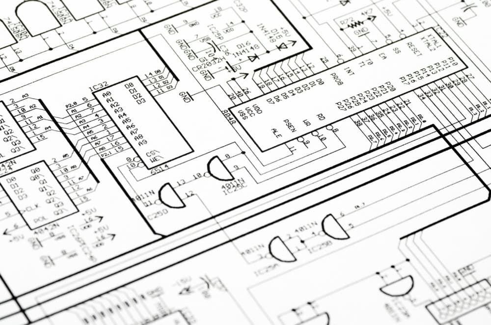
Especially for complicated digital and analog circuits, an electrical schematic design checklist can be vital to reduce errors.
When you are ready to transition from schematic to a PCB layout, it's important to ensure that you’re actually ready. For this reason, we've compiled an electrical schematic design checklist to consult before proceeding to the layout stage. Understanding an effective electrical schematic design checklist is best achieved by grouping list items according to common attributes
Schematic Set-up, Symbols, and Drafting Checklist
Rather than direct electrical connections, this table focuses on the layout of the ECAD software used, symbols, and naming conventions.
|
Section
|
Checklist Item
|
|
Set-Up and Rules
|
-
Has a grid size been chosen? Make sure pin placements align with the chosen grid size.
-
Is the Design Rule Check (DRC) configured and ready?
-
Arrange schematics to ensure readability from left to right, with inputs positioned on the left and outputs on the right, facilitating a natural flow of signals across the page.
-
Have the paper sizes for the schematics sheets been determined? Maintain consistency in page size across all schematic pages.
|
|
Symbols
|
-
Indicate internal terminations explicitly.
-
Check for consistent marking of active-high and active-low signals.
-
Clearly label any internal pull-up or pull-down resistors.
|
|
Drafting
|
-
Avoid using decimal points in values to prevent misreading.
-
Maintain all text orientation as horizontal for uniformity and ease of reading.
-
Avoid overlap among text, notes, references, wires, and symbols to ensure clarity and readability.
-
Confirm that every component is labeled with both reference and value for identification and value clarity.
-
Use standard designators for component references and place them unambiguously to avoid confusion.
-
Verify that all connections and markings serve a purpose, eliminating unnecessary elements for schematic cleanliness and focus.
-
Ensure that all appropriate power nets (Vcc, Vss, Vdd) are correctly connected.
-
Place net names directly on top of their corresponding lines for clear identification.
-
Terminate all unused inputs to prevent floating inputs and reduce noise.
-
Label all no-connect pins on ICs as NC to clarify intentional non-use.
-
Use 0-ohm resistors to connect mode pins or no-connect lines to GND/VCC for flexible PCB rework options.
|
|
Naming Conventions and Labeling
|
-
For clock signals, include the frequency within the name (e.g., CLK20_VCXO for a 20MHz VCXO).
-
Indicate negative logic signals with a suffix _N (e.g., RESET_N)
-
Number components sequentially and simply, using formats like C1, C2, R1, R2 etc.
-
Mark resistor values in a clear and standardized manner: use the plain number for ohms (49 for 49 Ohm), a letter for decimal places (4R9 for 4.9 Ohm),
|
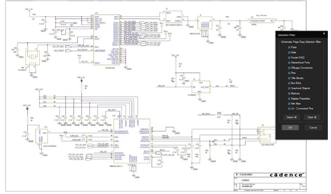
OrCAD X Capture CIS with consistent designator naming, grid-size, arranged for readability, and appropriate paper size.
Electrical Schematic Design Checklist for Signal and Power
This table focuses on signal integrity, noise suppression, grounding, and component protection.
|
Section
|
Checklist Items
|
|
Signal Integrity and Noise Suppression
|
-
Is there adequate decoupling to minimize power supply noise on ICs?
-
Do input signals from outside the board have appropriate impedance levels?
-
Are ferrite beads installed on power input/output lines to suppress high-frequency noise?
-
Are high-speed single-ended digital signals damped with series resistors?
-
Is there provision for a common-mode filter on high-speed differential signals?
-
Have op-amps been designed with input filters to reduce EMI?
|
|
Power Integrity and Regulation
|
-
Verify the stability of each switched-mode voltage regulator through simulation.
-
Ensure through simulation that each switched-mode voltage regulator maintains the necessary output voltage.
-
Implement sufficient input capacitance on each regulator.
-
Assess if any input voltages to regulators risk falling below minimum operating voltage.
-
Provide sufficient power rails for analog circuits.
|
|
Grounding Practices
|
-
Is filtering implemented between analog and digital grounds to prevent noise transfer?
-
Ensure no unintended ground connections exist between isolated sections.
-
Avoid power or ground loops to prevent interference and potential damage.
|
|
Component and Circuit Protection
|
-
Are optocouplers accompanied by filters to eliminate noise?
-
Do sensitive signal lines also utilize ferrite beads for noise reduction?
-
Are all ferrite beads rated with a sufficient margin for DC current to prevent saturation?
-
Analyze protection circuits for signal paths, focusing on current flow paths to ensure components are safeguarded against overcurrent and ESD.
-
Are all resistors verified to operate within their designated voltage range?
|
|
Signal Processing and Management
|
-
Confirm both positive (_P) and negative (_N) signals are employed in differential pairs and verify their polarity is accurate.
-
Is the reset signal properly filtered to avoid unintentional resets due to noise?
-
Is there a pull-up resistor on every open-collector output to ensure proper signal levels?
-
Consider the placement of a linear regulator downstream of any switched-mode sources feeding devices that demand exceptionally clean power.
-
Select high PSRR regulators for sensitive circuits.
|
 IC clock in OrCAD X Capture CIS, with appropriate naming and drafting, and frequency displayed for easy readability.
Integrated Circuits and Passive Components
This table focuses on individual components, including passive and active components.
|
Section
|
Checklist Items
|
|
ICs
|
-
Evaluate external accessibility for reading/writing flash/EEPROMs via connectors in prototype stages.
-
Assess the adequacy of decoupling capacitors for each IC to prevent noise interference.
-
Is there a provision for breaking out extra pins from ICs or subsystems for future expansion or testing?
-
Have all pins on each integrated circuit (IC) been accounted for in the design?
-
Identify if programmable devices include accessible programming headers/pads, especially for prototypes, to facilitate programming and debugging.
-
Are multipart components clearly identified and effectively utilized within the schematic to optimize functionality?
-
Examine each IC connection for correct implementation, especially hard-wired settings like division/amplification factors and operating modes, and annotate these on the schematic for clarity.
-
Evaluate global decoupling strategies for power supplies, such as the placement of large capacitors at power entry points or generation sites.
-
Have all necessary inputs been protected against Electrostatic Discharge (ESD)?
-
Are all pins of unused comparators tied to a common point to ensure stability?
-
For unused operational amplifiers (OPAMPs), is the output connected to the negative input, and is the positive input grounded?
-
Are all reset pins correctly pulled to their required high or low state to ensure reliable operation?
|
|
Passives
|
-
Check electrolytic and tantalum capacitors for reverse voltage tolerance to avoid damage.
-
Place a decoupling capacitor adjacent to each power pin on connectors to mitigate power supply noise.
-
Check the correct orientation of diodes and LEDs to ensure proper functionality.
-
Calculate the current through each resistor to verify power dissipation is within component ratings.
-
Check that each resistor, particularly in sizes 0402 and smaller, has a voltage rating sufficient for the maximum voltage applied.
-
Inspect the polarity of capacitors, especially those connected to negative power supplies, to prevent damage.
-
Ensure I/O pins include pull-up or pull-down resistors to define a default state when disconnected, enhancing circuit stability.
|

Schematic with BUS names automatically generated by OrCAD X Capture CIS.
Data-Related Items
Anything involving data, logic, buses, and digital components is discussed below.
|
Section
|
Checklist Item
|
|
Buses
|
-
For buses, align bus order with device order to simplify design and debugging.
-
Verify that all bits of buses are utilized to ensure full functionality.
-
I2C: Ensure pull-up resistors are installed on both the SDA and SCL lines.
-
JTAG: Consult the datasheets for any required pull-up or pull-down resistors to ensure proper functionality.
-
SWD: Again, refer to datasheets for the implementation of necessary pull-up or pull-down resistors. Why is accurate datasheet consultation important here?
|
|
Digital and Logic
|
-
Confirm each IC has a defined power-up state to avoid unpredictable behavior.
-
Implement filters on every Analog to Digital (A/D) converter pin to reduce noise interference, ensuring accurate digital representation of analog signals.
-
Implement pull-ups on all open collector/drain outputs for defined logic levels.
-
Incorporate capacitance and/or Zener diodes at the output of each operational amplifier to protect against voltage spikes and stabilize the output signal.
-
Verify oscillators for reliable startup, ensuring consistent timing functions.
-
Evaluate amplifiers for stability to prevent oscillation or distortion.
-
Assess op-amps used as comparators for appropriate time delays and slew rates.
-
Verify that all signals input into logic devices do not exceed the devices’ maximum voltage rating to avoid damaging sensitive digital components.
-
Confirm signal level compatibility across different outputs and inputs (e.g., LVTTL) to avoid logic errors.
-
Check op-amps for acceptable common mode input voltages to maintain linearity.
-
Select baud rate-compatible clock sources for devices with serial communication ports.
|
|
EMC
|
-
Assess if electrically noisy pins should be treated as pseudo-differential pairs for improved signal integrity.
-
Determine if long cable connections require isolation measures to comply with EMC (Electromagnetic Compatibility) standards.
|
Reliability and Validation
Finally this table focuses on checklist items after the major schematic has been made.
|
Section
|
Checklist Item
|
|
BOM
|
-
Evaluate if any component values across the design can be standardized to reduce the number of unique items on the BOM.
-
Specify only one part number for each passive component value of a given size to simplify procurement and inventory management.
-
Confirm that each specified component is readily available in the supply chain to avoid production delays.
|
|
Reliability
|
-
Assess the impact of input voltages when power is off, including CMOS latch-up risks.
-
Calculate maximum power dissipation at worst-case temperatures to determine heat-sink needs.
-
Examine the consequence of losing ground connections on multi-ground connectors.
-
Ensure automotive-powered devices can withstand voltage surges between 60 to 100 volts.
-
Monitor for voltage transients and high voltages on FET gates to protect against damage.
-
Estimate total worst-case power supply current to ensure supply adequacy.
-
Confirm resistors operate within their power rating, including a safety margin, for longevity.
-
Avoid driving tantalum capacitors with low impedance sources to prevent failure.
-
Prevent reverse base-emitter current/voltage in bipolar transistors to ensure proper function.
-
Ensure the schematic design compiles and passes all design rules checks (DRC) without errors.
-
Verify the inclusion of an LED indicator for each power rail, particularly at the input, to visually confirm power presence.
|
|
Testing
|
-
Are there designated ground connection points for testing equipment, such as probes?
-
Have test points been strategically placed to facilitate easy access to critical signals?
-
Provide a means to disable the watchdog timer for in-depth testing and diagnostics.
-
Enable power isolation for specific design sections to facilitate targeted testing.
-
Incorporate diagnostic resources (LEDs, serial ports, etc.), even if unpopulated by default, for troubleshooting.
-
Include test points on power and ground lines for comprehensive system testing.
-
Are configurable strap-in pins set to a default logic level through biasing?
-
Are configurable strap-in pins equipped with jumpers or similar connectors for easy configuration?
|
OrCAD X is your ultimate partner in schematic design and validation checks. With its advanced features tailored for all stages of PCB design, OrCAD X streamlines the process. Sign up today for a free trial of OrCAD X.