PCBA Design Tips to Avoid Reflow-Induced Failure
Key Takeaways
-
What is reflow soldering?
-
What types of reflow-induced failure can occur during assembly?
-
How to design your PCBA to prevent failures during reflow.
Conveyor reflow oven.
To generate any tangible item of any degree of complexity, there are four essential requirements: First, is a clear plan or strategy. Second, is the knowledge or expertise necessary to execute the plan. Third, is possessing the necessary tools or equipment. And, finally, you need the time to integrate the previous three. Armed with these essentials, virtually anything can be accomplished or produced. However, the quality of the result is often determined by the specific equipment and how effectively it is utilized.
PCBA development is a good example of how these four aspects of product generation are implemented. The process begins with and depends upon a well-defined design that includes specifying all materials, components, and their arrangement, or the stackup and PCB layout. The design embodiment is finalized with the utilization of PCB assembly equipment to place and securely attach components. For surface mount components, along with pick and place, reflow is the most important stage.
Let’s first define reflow soldering and then investigate how to best design boards to avoid potential reflow-induced failures that can threaten successful PCBA development.
What Is Reflow Soldering?
Let’s start with a definition:
Reflow soldering is a surface mount technology (SMT) process for attaching components
to a PCB’s top layer, and for two-sided boards, the bottom layer as well. The process
involves running the board through an oven where it goes through a four-stage profile:
preheat, soak, reflow, and cooling. The temperatures and time intervals for the stages are
preset based on parameters that include: board size, number of components, number of
layers, type of solder, etc.
As stated above, reflow soldering is used to secure SMDs to the circuit board during assembly. The reflow stage of circuit board assembly is a thermodynamic process where the board is subjected to a range of temperatures over four intervals, as shown in the figure from [1] below.
Infrared reflow profile.
(Alt text: A graph of the reflow soldering stages)
IMG: IR-reflow-temperature-profile.png in Cadence | Software Images | PCB Manufacturing | Assembly.
The temperatures shown for the reflow profile above are typical for the solder pastes in use most often by PCB contract manufacturers (CMs), with the peak for leaded solder at approximately 210-220°C and lead-free solder about 30°C higher. It should also be noted that the temperature for the dry-out or soaking stage is ideally fairly constant. This is also true during the reflow stage as the temperature should be at or above the desired peak temperature for a fixed preset duration. Not adhering to the proper temperatures or time intervals can lead to failures, as discussed below.
Potential Failures When Soldering SMDs
Although the through-hole soldering process can have challenges, these pale in comparison to the reflow-induced failure possibilities. Possible issues range from poor solder joint quality to component and/or board damage. These and other contingencies are listed below.
TYPES OF REFLOW-INDUCED FAILURE
-
Oxide creation - can occur when oxygen is present during reflow.
-
Solder balls and/or beads - can result from insufficient heat.
-
Graping - due to exhausted flux.
-
Head in pillow - may occur with excessive soak temperature or interval.
-
Component cracks - caused by a heating rate that is too fast.
-
Board warping or breaking - due to pressure applied after board weakening during reflow.
As listed, the above contingencies occur as a result of imprecise reflow soldering execution; however, there are design factors that contribute to the board’s susceptibility to these failures. Fortunately, these can be avoided, as we discuss below.
Design Guidelines to Prevent Reflow-Induced Failure
In many cases, reflow-induced failure means that unusable boards are being manufactured, which can translate into longer turnaround times and increased manufacturing costs. Yet, by instituting a design-to-value approach, that includes making decisions that aid your CM in the assembly of your boards, as shown below, these manufacturability contingencies can be largely mitigated.
How to Avoid Reflow-Induced Failure
☐ Balance copper distribution on board.
☐ Ensure PCB trace routes connected to components are similar in size.
☐ Select high-quality components without vulnerabilities to reflow temperatures.
☐ Make sure there is adequate spacing between board elements.
☐Make good use of thermal paste and other heat transfer techniques, if needed.
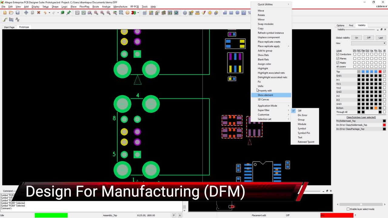
☐ Follow good design guidelines for footprints (as described in the video below).

Example footprint design with Allegro PCB Editor.
By following the tips listed above, and instituting all DFM rules and guidelines, you can best assist your CM in making sure that your development does not suffer from any reflow-induced failures.
The best way to avoid the potential additional costs and extended time for development that reflow-induced failures can cause is with a highly capable software tool such as Cadence’s PCB Design and Analysis package. The capabilities of Allegro PCB Designer, coupled with the advanced thermal analysis functionality of Celsius Thermal Solver, help you to create a design optimized for PCB assembly.
If you’re looking to learn more about how Cadence has the solution for you, talk to us and our team of experts.
References
1. Pecht, Michael. (1999). Moisture sensitivity characterization of build-up ball grid array substrates. Advanced Packaging, IEEE Transactions on. 22. 515 - 523. 10.1109/6040.784506.