Managing Interconnect Density and Signal Noise
Key Takeaways
-
Trace spacing and density need to be examined alongside trace inductance in a high density board.
-
Depending on the layer stack and trace width in your board, you may be able to violate the 3W rule if the loop inductance and coupling capacitance are small enough.
-
Signal integrity simulations should be used to examine crosstalk strength between two signals in a PCB layout, as well as susceptibility to external EMI.
Do you know the right interconnect spacing and density you should use?
If you’re a seasoned PCB designer, then you know all about the ‘3W’ rule, which states the spacing between traces should always be at least 3x the width of each trace. This antiquated rule says nothing about your stackup or loop inductance, but many designers still cling to this rule. With HDI boards being pushed to smaller sizes and higher density, such as in baseband chips with 6 mil traces, the strength of crosstalk and interconnect noise coupling between traces will depend on the spacing between them. This means you need a way to quickly evaluate crosstalk and EMI susceptibility in your board as a function of interconnect density.
When you’re designing your PCB, you need to perform these simulations and analyses post-layout. In other words, your schematic editor cannot consider the physical layout of traces and components, so it cannot be used to simulate anything related to stackup, trace size, or trace density. Circuit simulators in your schematic editor still have their place in circuit simulations, but managing interconnect density requires determining noise coupling directly from your layout data.
With the signal integrity simulation features in Sigrity, you’ll have the tools you need to examine crosstalk and broadband signal reflection in real interconnects with an integrated field solver. These tools are accessible within your layout, and you’ll have the ability to analyze crosstalk on specific nets, including differential crosstalk in closely spaced traces. Here’s what you need to analyze when you need to prevent interconnect signal noise coupling.
Understanding Interconnect Inductance, Crosstalk, and EMI
Your next board will need to balance a number of different geometric requirements to prevent crosstalk between single-ended and differential traces. The difficulties in highly dense boards arise simply because the electromagnetic field emitted from a trace is stronger when you are closer to the trace. The lower-frequency portion of a broadband signal will couple to a nearby trace inductively (through the magnetic field), while the higher-frequency portion of a broadband signal will couple to a nearby trace capacitively (through the electric field).
Crosstalk
When managing interconnect density, you need to consider how different types of signals couple to each other. Single-ended and differential pairs couple with other types of traces in a variety of ways, and the table below shows a summary of the results you would expect from a signal integrity simulation. Note that in the single-ended → differential pair crosstalk result, the presence of either common mode or differential mode noise depends on the values of spacing between traces in the victim differential pair (S) and the height of the pair from the ground plane (H).
In the above table, we’ve assumed that all single-ended traces and differential pairs sit on the same layer (i.e., no broadside coupling). This is the common situation you’ll need to simulate in most layouts. A less common arrangement is broadside differential pairs, which can experience strong crosstalk when placed close together. In all cases, crosstalk between differential pairs will be weaker than crosstalk between comparable single-ended traces, and crosstalk strength will be weaker as the separation distance increases.
Thanks to the rise time of commercially available digital circuits, your trace inductance will dominate crosstalk given the relevant signal rise times in most digital systems. However, everyone should expect signal rise times to continue decreasing to accommodate higher data rate channels (e.g., 800G and higher SerDes), which may push useful signal bandwidths closer to 100 GHz. At some point, capacitive crosstalk will need to be considered in your system alongside inductive crosstalk.
Quantifying EMI
The same geometry constraints will also influence the board’s susceptibility to external EMI. The inductance of signal traces in your board determine their susceptibility to external EMI. Inductively coupled EMI arises from the magnetic field from an external source, which can be a broadband signal. External EMI sources, such as another board in the system, can emit strongly at discrete peaks; poorly isolated clocks and high current switching power supplies are prime examples.
EMI is coupled as common mode noise on single-ended and differential nets in your board. The noise coupled into a trace can then propagate through either linear or nonlinear components, which can then generate noise at higher harmonics. The complicated feedback between induced noise and signal integrity can be difficult to simulate conveniently. However, your goal should be to minimize EMI by minimizing loop inductance in critical nets in your board.
Whether you are worried about crosstalk or EMI in your board, you can use a post-layout simulator to examine how noise transfers between board regions as a function of geometry. Here’s how this works in Allegro Sigrity SI and how you can import boards directly from Allegro into a simulation instance.
Simulating EMI and Crosstalk vs. Interconnect Density
You can create crosstalk simulations before or after you finish your layout. In my opinion, it’s best to create a test board with two interconnects on a PCB with only a single driver and a single receiver. If you route the traces side-by-side, you can use the simulation tools in Sigrity to calculate crosstalk between the interconnects. You can then vary the distance between the traces, the width of the traces, and the layer stack to determine how each of these parameters affects crosstalk strength.
When you’ve produced the ideal waveforms from your simulations, you can move on to routing your board. Once you finish your PCB layout, you can finish your board with another round of simulations on critical nets. The goal in both cases is to determine the appropriate trace density for single-ended and differential nets. After you determine appropriate clearances in the first round of validation simulations, you can then set your appropriate trace spacing and differential pair separation as design rules, and Allegro will follow these design rules as you layout your PCB.
If you can prepare a graph such as the one shown below, you’ve done a lot of the hard work in preventing crosstalk before you’ve even completed your layout. In this graph, a single limiting frequency was used (2 GHz) with fixed layer separation and trace thickness. Increasing the layer separation will move the curves up the graph as loop inductance would increase.

Crosstalk vs. interconnect spacing. [Source]
EMI can be more difficult to summarize in such a simple graph as the results you’ll see can be complicated functions of frequency and geometry. However, with the right simulation tools, you can examine susceptibility to EMI and crosstalk strength throughout your PCB.
Creating Interconnect Signal Noise Simulations
When you’re in Allegro Sigrity, you can access crosstalk simulations from the Analysis Workflows tab in the main Allegro Sigrity SI window. The group of differential pairs shown below is a prime candidate for a crosstalk simulation. To get started, you’ll need to select nets by name as you set up the simulation.

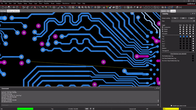
Bring up your board in Sigrity for an interconnect signal noise simulation.
The other important point to setup in the analysis is the region around each net that will be included in the analysis. If you click the “Analysis Options” entry in the Analysis Workflows tab you can set the size of the simulation region around each trace using the GeoWindow option.
Once you’ve defined your settings, the tool returns results that are compared against your design rules. The results are color-coded and arranged in descending order. Although these are color-coded, you can also see a numerical result so that you can compare the peak overvoltage/undervoltage due to interconnect signal noise and compare these with your signaling standard.

Interconnect signal noise coupling (crosstalk) simulation results seen at the receiver for an LVDS component (3.3 V differential voltage required at the receiver).
When we look specifically at the LST_RESET net, we see 3 aggressor traces that produce crosstalk on this net.

Interconnect signal noise graph on a victim trace.
In this net, the solution is to modify the spacing between the victim trace and the aggressor traces. Because 3 traces are involved in producing this level of interconnect signal noise, it can be difficult to determine the best trace arrangement. Moving the victim trace away from one aggressor may require moving it closer to one of the other aggressors. In this case, you should experiment with different arrangements and rerun the simulation to determine the arrangement that minimizes crosstalk.
There are other important simulations you can access in the Analysis Workflows tab in Allegro Sigrity SI:
-
Impedance workflow: Examine impedance discontinuities and variations along a trace due to coupling under common-mode or differential-mode driving.
-
Coupling workflow: Extract coupling coefficients between different nets, which will determine even and odd mode impedances.
-
Reflection workflow: Examine reflections from a receiver due to minor impedance mismatches.
-
Return path workflow: Examine the return path for signals in single-ended nets.

To learn more about all things interconnect density, signal noise, and other high-speed necessities, read through our free ebook today.
If you’re looking to learn more about how Cadence has the solution for you, talk to us and our team of experts.