Home
Free Trial
Home
Free Trial
Read More
Content
Filter
10 results found
Featured
OrCAD X High-Speed Digital Design Guide Part 2
Featured
OrCAD X High-Speed Digital Design Guide Part 3
Featured
RF Via Transitions in High-Speed Designs
Featured
HDI PCB Design Guidelines
Featured
OrCAD X and Allegro X
Featured
OrCAD X: Create Symbol Capabilities
Featured
OrCAD X Free Viewer
Featured
To Design For High Speed Data Rates
Featured
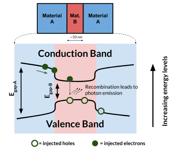
Quantum Well Design Basics
Featured
The Co-Fired Ceramic Fabrication Process
Featured
Products
None
OrCAD X
(3)
Allegro X PCB
(1)
Sigrity X Aurora
(3)
Content types
None
Design Guide
(2)
Blog
(8)
Solutions
None
PCB Layout
(7)
Schematic Capture
(2)