Sustaining Engineering - What to do After You Hit a Homerun
By John Burkhert Jr
Success! Oh, the sweet, sweet problems of success. The first problem is that we just cannot build these (insert product) fast enough. The second is that suddenly there is a new cash cow in the room. The people with more business savvy than me, as evidenced by the nicer desk locations, want to further milk that cow. As they pour over the costed Bill Of Materials, the thing that always seems to stand out is the Printed Circuit Board. Well, PCB's do not grow on trees. How do we plant a seed that brings the unit price down?
Image credit: author -The frame replaces most of the typical component keep-out for the assembly rails.
Capture the story
Start by writing a book about it. Call it a handbook, an Assembly Handbook and it will seem less daunting. The plot of the book is simple; make things. The characters come from all over including the 3-D model, the CAD tool, a marked-up assembly drawing, photos of the real board with a real jumper wire and so on. If you do not see this being done already, create a cross-functional team with the idea of bringing this document into existence. The goal is to provide a baseline for a traveler, a document that follows a lot of boards through the factory.
It all begins with kitting a work order. This is the stage where a stock clerk fills a bin with reels of components and a stack of bare PCBs. The bin is made of special material that dissipates static charges. Special areas of the plant are set aside for the application of solder paste. The circuit is fleshed out on the pick and place machine with astonishing speed and accuracy. Document everything. It might take more than one set-up if the parts mix exceeds the capacity of the robot in terms of the number of different reels required. Shorten the bill of materials wherever possible.

Image credit: Author. This assembly array panel has an A-B flip such that one paste stencil works no matter which side is up.
2nd act
The next chapter follows the PCB into the system and covers all of the hand operations. People scrutinize the assembly and certify it ready for shipment or up the integration chain to a final product. Or not. Everything, including the solder profile, paste composition, stencil thickness and so on should be documented.
This effort is entirely apart from the assembly drawing. This is the how-to, not the what-is. The assembly drawing characterizes an acceptable assembly. It is not about how you get there. That is where these process documents come in. Doing all of this dry documentation while working with the Manufacturing Engineer may seem tedious. Do it anyway.
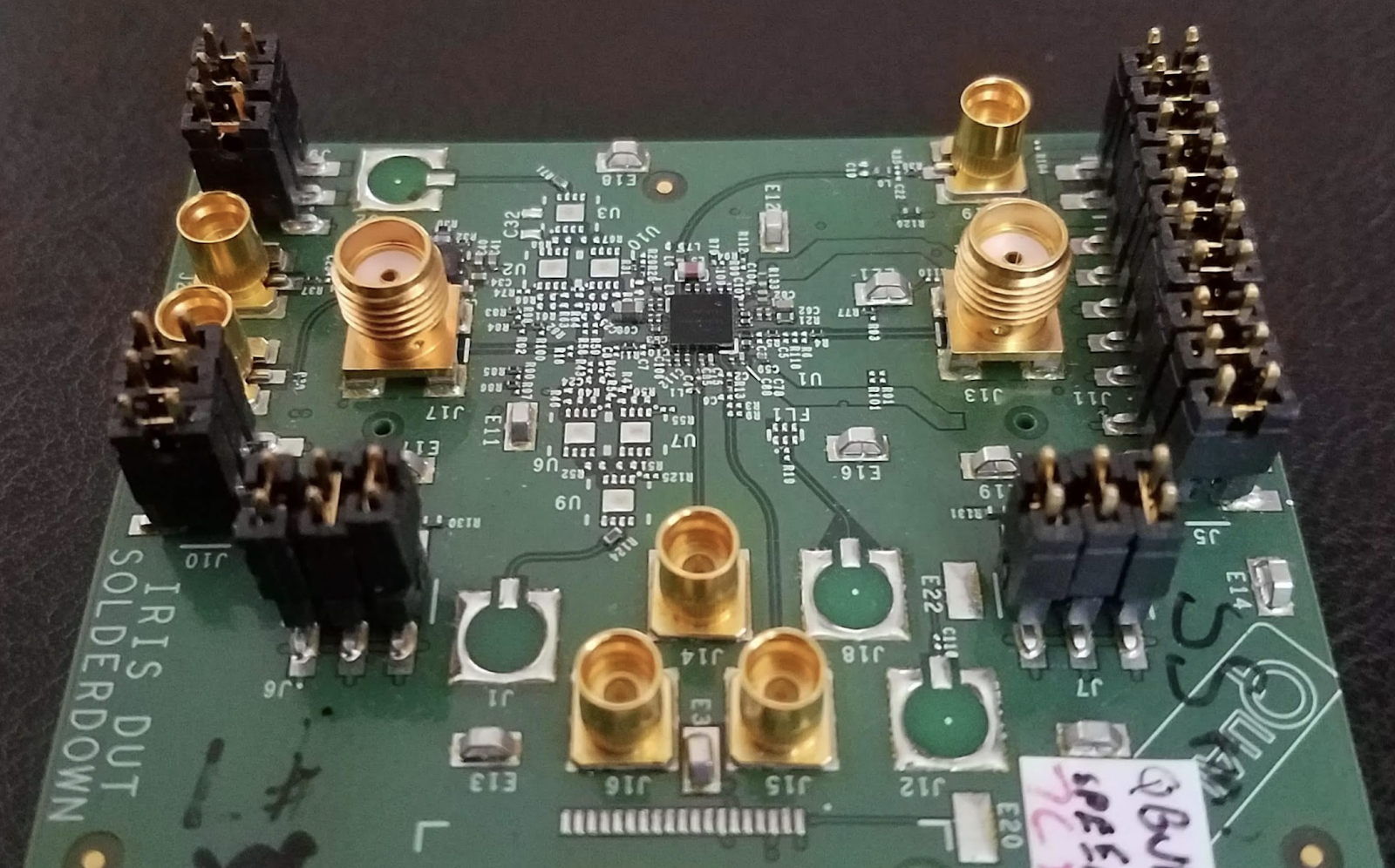
Image credit: Author - DUT stands for Device Under Test. A socketed version would be used for screening and flashing memory.
It is very much worth the effort in the long run. Learning about their pain points and driving/documenting the solutions will make you a pivotal part of the larger team. PCB Design lives in the space between the chips and the final product. Pushing into the small and large ends of the overall picture makes us more effective. If nothing else, be prepared to generate a few images for the app notes.
Work and more work
Let's switch gears for a moment. In theory, long-term planning should smooth out the workflow so the peaks are lower and the troughs are shallower. Still, there is going to be a peak followed by some quieter time between chip-sets or whatever may define the next wave for you. In a typical design flow, all development ceases as soon as the mass production starts. Further changes would have to be re-qualified or retooled and it is not going to happen. This time. Never say never though. Showstoppers can become visible well after the production start date and so, we may revisit the previously 'frozen' data in another rush.
Clean-up time.
The first thing I do after the final revision is released is to branch into the next revision. Nobody is asking for it and sometimes they never do. If there is a problem, the bucket for that data already exists. As-built stack-ups or line widths can be incorporated here. Exceptions to the notes and tolerances or even the solder mask color can be specified to distinguish prototypes, pre-production and mass production. Color coding comes in handy around the lab with so much gear around.
Image credit: Author - System test fixtures are a staple of the manufacturing floor. Good labels help avoid mistakes.
No stopping there though. Some boards are designed on a tight timeline and are conservative on the layer count. Perhaps, a few shortcuts were taken with the library. We may be able to increase the capture pad size for the vias to open up the process window. On the other hand, maybe the time is right to consider a more technical solution that shrinks down the overall size.
The project's original goals will help establish the potential upgrade path. If the goal is to reduce cost and/or increase performance, then investigating the available avenues while the PCB design is out of the spotlight is good practice. Even if the uptake of the effort is not 100%, checked footprints and design insights gained by the experiments are positive outcomes.
Shopping around.
Circling back to the B.O.M., the product lifecycle is long enough that there is always a risk that a device will be discontinued or that the price and lead time become untenable. Drop in replacements can be considered a lucky break for anything beyond value changes among the capacitors and resistors. Cutting in a new footprint is the main reason we get to see a revision B. Fixing an EMI issue is number two.
Good buyers continue shopping around when the volume demands the scrutiny. The math varies so the numbers are made up. If an ECO costs $10,000 and the unit cost drops enough that the projected savings is $15,000, then that improvement can be sold to management. If it takes two iterations, it is a net loss. That is the thing. It pays to be fastidious about accuracy on the re-spins. Mass produced scrap has buried more than one factory.
Of course, you will have other work on your plate. Supporting the factory will take a few hours per week; not enough to derail the next new product introduction. There are times when it is good to let a project rest if only for a moment. Switching gears may seem like an inconvenience but it allows us to get away from the day-to-day work and do some vital networking. Keep an eye on the big picture and milk that cash cow all the way to the bank.