Unpacking Logic as it is Used on a Printed Circuit Board
The truth shall set you free. The truth table of a logic device will determine the outcome of a logical operation. There are a handful of operations that are described as gates. The gates are named for the function that applies. Two main ones to start with are the AND gate and the OR gate. Both of these usually have two inputs and one output.
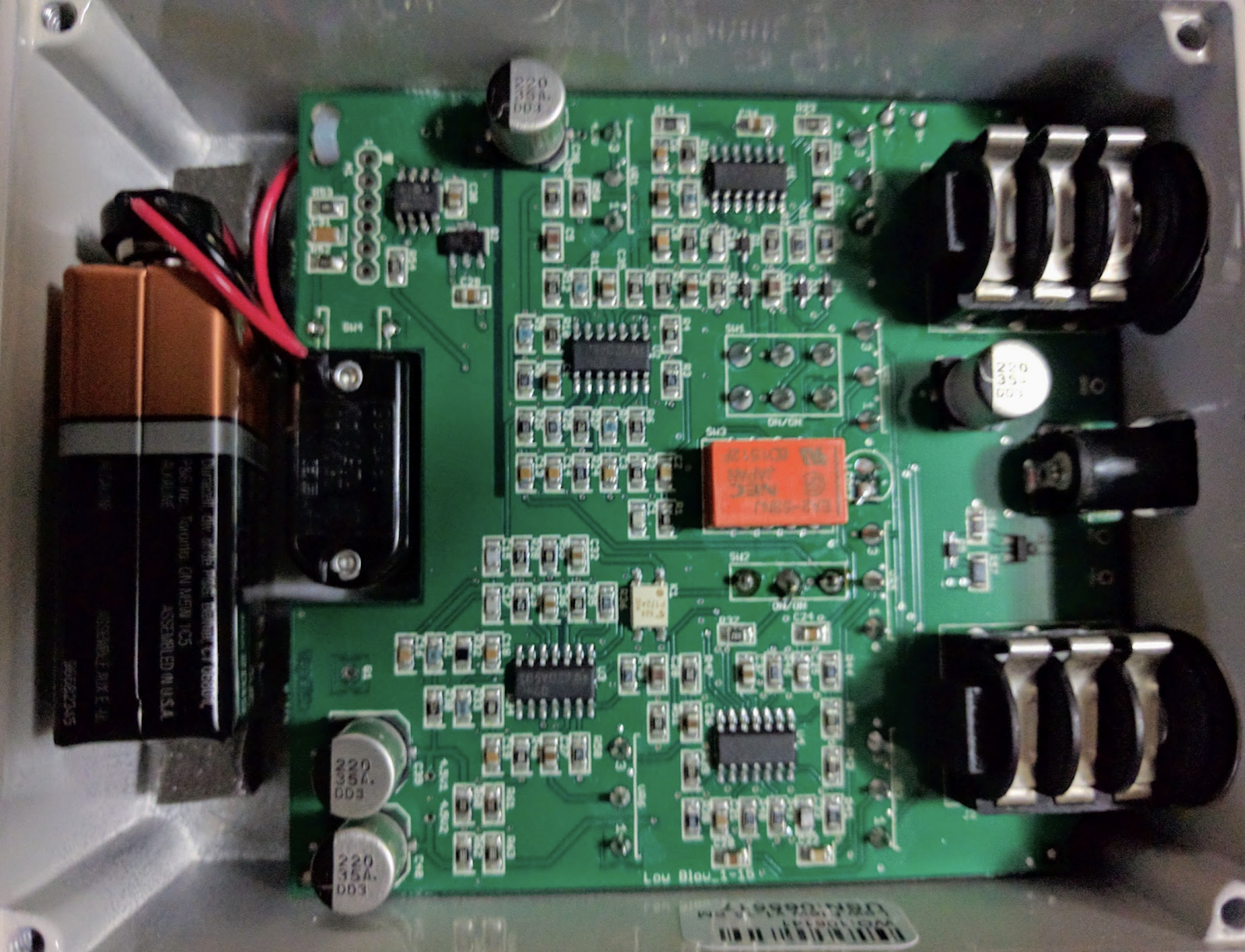
Figure 1. Image Credit: Author - Guitar effects pedal Small signal processing carried out with the help of basic logic devices.
You may have a hallway or stairwell light in your home where there is a light switch at either end of the passage. When both switches are in the down position, the light is on. When both are up, the light is also on. If one is up and the other is down, the light is off. The truth table for those two switches would be as follows:
| SW1 | SW2 | Result |
| On | On | On |
| On | Off | Off |
| Off | On | Off |
| Off | Off | On |
We represent the binary logic states with a One or a Zero though there are exceptions. The One can also be called High state while the zero would represent a Low logical state. One or Zero, High or Low, Voltage applied to the pin or not applied are all ways of describing the situation. Low is not always synonymous with ground. It could be a negative voltage. Some devices can have a tri-state output that uses negative and positive voltages with ground as the middle state.
Turning Code Into Action - The Abstract Becomes Concrete
Setting that little wrinkle aside, machine language is a string of Ones and Zeros that are compiled from a list of logic statements in the software. Once compiled, the binary code can be applied to the logic gates to do something useful or at least amusing in terms of manipulating the input to drive an outcome.
In order to activate an AND gate, both of the input pins must have a voltage applied. An OR gate only needs one of the input pins to have a charge but a positive outcome can be had with a nominal voltage applied to both input pins. If we didn’t want a high state when both pins of an OR gate are active, we could use an Exclusive OR gate also known as an XOR gate.
Furthermore, we could flip the bit so that all of the outcomes are reversed. Put an N on the front of the descriptor for a NAND and a NOR gate. The OR gate can be both exclusive and inverted which we call an XNOR gate. The two light switches that I mentioned up above resemble the EX-NOR circuit. They are also very useful in memory devices.
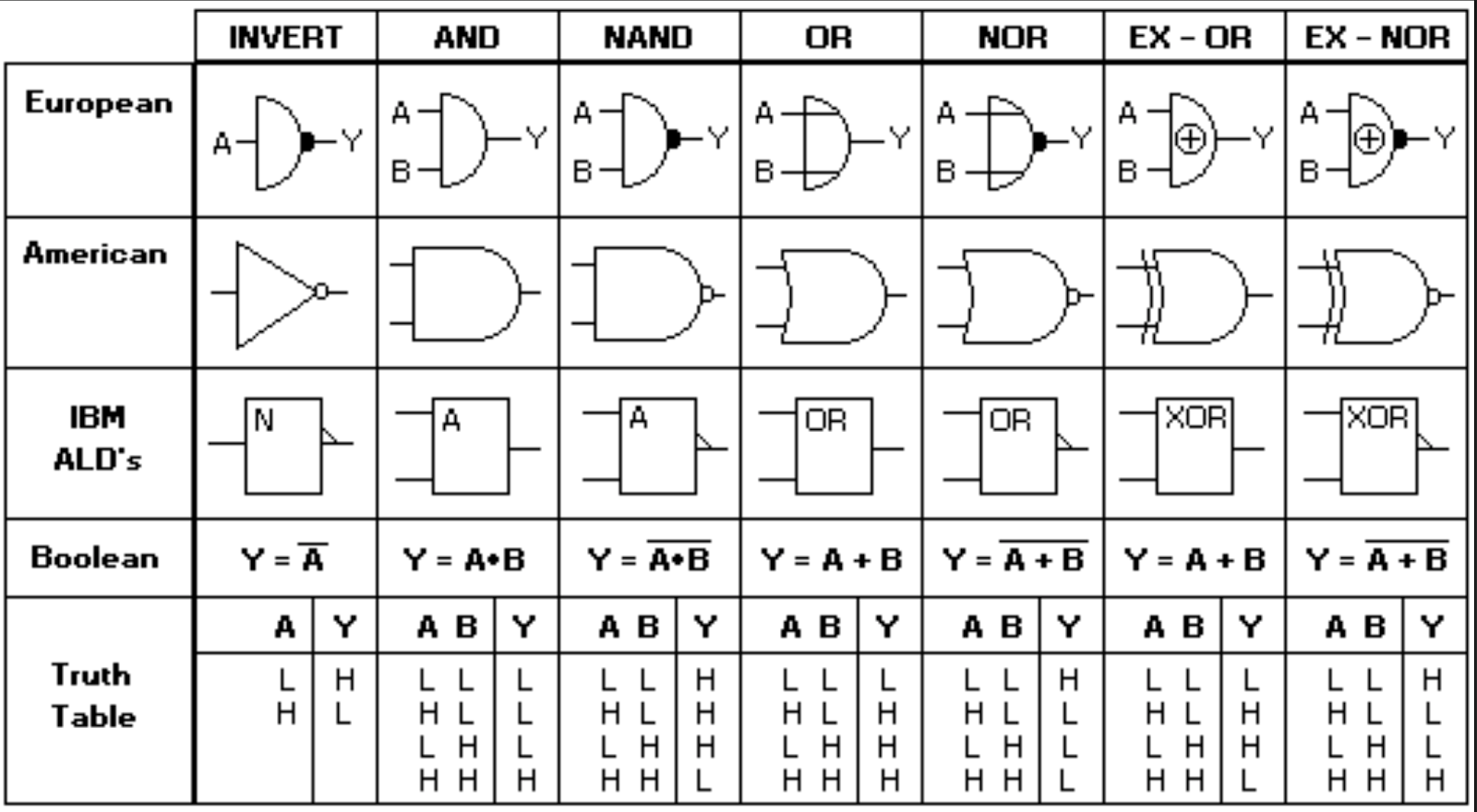
Figure 2. Image Credit: IBM: A visual of the schematic symbols and truth tables of typical logic gates.
Buffers and Inverters: More Useful That You Might Think
Fleshing out the other simple logic gates are the Inverter and the Buffer. These logic devices have one input pin and one output pin. As you’d expect, an Inverter will flip the bit from one state to the other depending on what comes in.
When it comes to a Buffer, the idea is to refresh the signal without altering the state so we can send it on its way. The Buffer may be useful as a means to revive the voltage to its full specification while removing any other signal integrity issues. The schematic symbol for the buffer is like the inverter except there is no little circle on the output pin. As you can see, the circle is common to all of the gates that invert the outcome.
The Evolution of Logic: Lower Power, Faster Switching
Over the course of time, the working voltage for logic gates has gone down. The smaller voltage swings happen faster with less switching noise. Back when I started out, we had TTL (transistor-transistor logic) which ran on +/-5V. Along came CMOS architecture and 3 is the new 5. It keeps on progressing. The data rate jumps while the voltage goes down. That progress means that the threshold between a Zero state and a One state is a little more difficult to read if there is significant voltage drop over a length of trace or wire.
That’s where those buffers come in. You could also create a buffer by chaining two inverters together in series. The output is refreshed while the double switch puts the logic in the original state. Since inverters typically come with six or more gates in a standard package, there may be a few empty slots somewhere to use for that purpose. You can be creative with these building blocks.
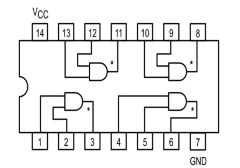
Figure 3. Image Credit: Circuit Digest - 4LS09 QUAD AND GATE Typical configuration in a 14-pin package has four logic gates or six in the case of inverters or buffers.
These primitives are themselves made of a small number of transistors and passive elements. The AND gate is not restricted to two input pins. It could take three or four input pins registering a 1 for the output pin to follow suit. There are other circuits that combine functions into more integrated features. You may have heard of a flip-flop (not the shoe), a level shifter or a comparator for instance. These are conveniently packaged groups of logic gates for specific purposes, of which there are many.
Gate Swapping - Because Nobody is Perfect at Schematic Capture
The first iteration of the schematic is unlikely to result in a totally smooth flow, especially when we allow the system to randomly assign the individual gates to their packages. Even when we try to plan ahead, the PCB layout may have areas where reassigning the logic gates is beneficial. That might be done by revisiting the schematic.
Another way is to optimize the connections while in the layout using a gate-swapping routine. First, you have to be sure that gate swapping is, in fact, allowed. Then you have to back-annotate the schematic to align with the layout. Your approach will depend on your normal tool-flow and the complexity/flexibility of the circuit.
These humble circuits have become cobbled together with others to form massive colonies with billions of transistor level residents. It all begins with statements written in software which is compiled into binary code that drives the whole process. The super-massive system on a chip is no more complex than this. It’s just that there is a lot of it all in one location. Have fun trying to keep up with our digital future.