02 - Controlling Trace Width Using OrCAD X and Allegro X Tools
Discussions of copper width and thickness are drawn from power and impedance requirements. These have to be filtered through the lens of what can be done by your fabricator’s production limitations. We have to pull data in for thermal considerations. Every part has a rating that it has to meet. Provisions for dissipating the expected heat build-up have to be included on the board. For the most part, we rely on what can be found in the schematic to help us set up design rules for signal integrity.
For things that we can’t discover for ourselves, engage with the cognizant engineer who is driving the project. They will know what is most important but there may be some disagreement if you’re part of a team project where people are competing for the most valuable PCB real estate. When the inevitable conflict arises, the written correspondence should carry more weight than spoken words. Of course, it always depends on whose words are in play. Either way, what is written is going to reflect what is done.
The most useful callout is noting the impedance on the schematic page while embedding the impedance value as an attribute given to the net(s). That would be nice. Of course, the name of the net(s) should also provide context for capturing the high-level design rules. Without those clues, you’ll rely on standards, component datasheets and application notes to provide the general guidelines along with all of the pin functions.
Knowing which traces get the treatment is only the start. Parsing that information into line geometry and dielectric thickness is part of your gig. The stack-up data and the constraint manager work together to form the virtual twin that drives the production of boards. There are tools that allow us to easily calculate stripline or microstrip models. The best data to use is the stuff you get from the fab shop that is going to eventually build your boards.
The usual flow is to take a shot at it yourself first. Propose a line width and stack-up to your vendor(s). They respond with something close to that but using numbers for the dielectric constant based on the material they use. That can vary by country but also by which of numerous PCB factories will be used by the ODM as you go to mass production.
This vendor feedback often requires a small update to your proposal. Depending on your relationship with your vendor (or the internal buyer) they may be up for generating the stack-up and all of the controlled impedance geometry layer by layer. This is really nice to have at the beginning of a project.
I have to say that there is also a school of thought where you give them your nominal data and describe what each line width means in terms of impedance. They give you the feedback and as part of the DFM cycle, you approve the deviations between the artwork and the physical board. If I’m using multiple vendors for a job, I’m likely to take this course. After working with a manager who saw technical questions from the vendor as a failure of the ECAD designer, I want to minimize the post-tape-out interactions. If you can get ahead by capturing the actual data ahead of time, it’s worth the effort.
The easiest way to get traction with a constraint set is to start with a mature board and export those constraints. In order to read it into the new database, the names of all of the etch layers must match. After enough years of doing this, I have some 8, 10 and 12 layer scripts that clean up old “vendor” designs so that they comply with layer naming standards. There will still be specific attributes to capture that align with the net names and other conventions of the current project.
Creating Bespoke Design Rules Tailored for Each PC Board
Maybe it’s the way I was raised but I want to start out with the analog nets and highlight those. A well-trained eye can pick out the RF traces from the antenna or connector through the matching network and right to the radio. Where there’s an input, there’s an output; sometimes more of one than the other. There’s something to be said for browsing through the data before jumping into the board design.
Refine those rules to the extent possible so that you have an easier time as the job proceeds towards tape-out. You may find that the component footprints leave something to be desired. If you don’t want to see copper pour under your inductors, you can create the voids after the fact once the ground copper is poured. A more efficient way is to put a route keep-out between the pads as part of the footprint. You draw one route keep-out and update the inductor (or whatever) so that every time you pour a new shape, it honors the keep-out regions for all instances.
The general idea is to capture design intent in a way that makes it less likely that a defect of some kind makes it all the way to tape-out.
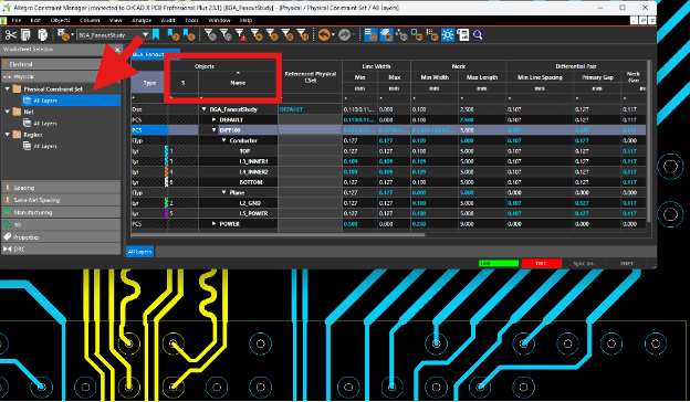
Figure 1. A slice of the physical constraint window where different classes of connections receive their width requirements. The red box indicates the location where we invoke the filter to narrow down the field.
Note in Figure 1, the DIFF100 class is expanded to show line width and air-gap for each layer type along with a neck-down width and gap for tight routing channels. All other air-gaps are controlled in the Spacing tab. The red box near the upper left-hand corner indicates the area where you can Right-Mouse-Click to access the Filter.
Just below the constraint manager is a bit of graphics that show what happens when you cross into a Constraint Region. Traces going south of the green Constraint Region outline automatically slim down to a preset regional rule. I would use those regions sparingly, affecting as few layers as possible.
The neck-down option is more flexible for trace widths. The regions are best for supporting dynamic copper where you can use a smaller air-gap in support of fine-pitch devices. I would start with the default rule set. It can be copied and modified to allow the shapes to close in on the other geometry. The trace widths would remain the same as the default rules unless that is going to be impossible to fan-out.
The idea is to maximize the copper web for the power and ground plane layers. Again, I would rather create constraint regions one layer at a time than the blunt instrument of an all-layer region. This gives us more latitude to handle exceptions.
The physical parameters also include the type of via to use. As an example, the BGA field in the Figure 1 image is populated with smaller vias than those outside. Support for stacking or staggering blind and buried vias is also supported in this window along with a true/false option that restricts routing to certain layers. The constraint manager spreadsheet is just too wide to show it all clearly.
The physical constraints are parsed three ways with the general rules first followed by net-specific details. The typical “detail” is selecting what type of trace technology to use from the general classifications but there are many options for constraining traces. Minimum Width is straightforward. The only issue is that it has to be less than the maximum - unless the maximum is set to zero. The zero means that there is no maximum so whatever width you choose in the PCB editor is allowable by the Design Rule Checker (DRC) just as long as it meets the minimum trace width. The third method of width control, beyond default and neck down, is to use a constraint region as mentioned above.
When I really want to control the line width for a trace on a given layer, I will set the Minimum, Maximum, and Neck width to the same value. If the line is any other width for a connection on that layer, a DRC flag will appear until the line is changed to the one and only value being allowed.
Taking this step allows us to prove that the RF traces are all the same as the specified width. The Physical Constraint Set has to have the same value in all three locations for the Minimum, Maximum and Neck modes. This is most important when you’re making a global change to the trace geometry and do not want to leave anything behind.
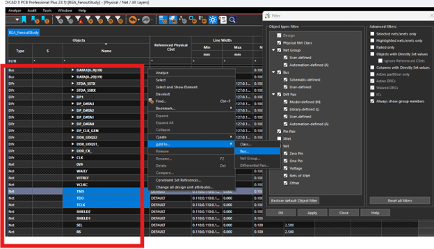
Figure 2. This is the “Net” folder of the Physical Constraint set.The red box now indicates the location for the Right-Mouse-Click to add a net (or three selected nets in this case) to a bus. Different tabs of the constraint manager allow for the creation of different types of groups depending on context. To the right you see the filter for simplifying the results.
Creating “rooms” for component placement is a good way of keeping component groups together. This method goes beyond what is in the group to include defining where the group would be placed on the board. The rooms can have assigned values for maximum height which would be useful for groups that live inside of a shield or other low headroom area. Of course, those areas are ripe for getting their own set of local design rules as well.
We set up the high level placement, known as floorplanning using critical routing and voltage domains as guidance. Floorplanning generally starts with the components in predefined locations, say connectors and heatsinks for example. Then, the larger integrated circuits are considered. For smaller circuits such as regulators, I like to create an ideal layout of the section off to the side of the board for a more informed placement before I bring that circuit onto the board.
Whatever group you’re creating, tracking them all down and giving them a highlight color allows us to use the filter to narrow down the field for adding additional design rules. The constraint manager shows all of the nets by default but you can click a box in the filter window and only the highlighted (or selected) nets remain for editing.
Also notice an option to display “Failed Only” that will surface the connections in need of improvement while hiding everything else. What’s the highest number of pages you’ve seen in a schematic? The filter is a good way to stay focused on design verification of a complex printed circuit board.
In spite of our best efforts, signal integrity and power integrity issues are still a risk. When something happens outside the scope of what the constraint manager covers, we’re asked what we can do to prevent a repeat of the situation. At this point, we need to review the available properties.
A shape can be given any one of over sixty properties. A component has seventy and a net can be given almost 300 different properties. Whatever is selected in the find filter will generate a different list of these attributes. Many of them are simply to get around a DRC that can’t be otherwise avoided.
Some of the properties overlap with the constraint manager. I can select a pin at large and add a rule about whether the copper will flood over the pin, create thermal spokes or ignore it by creating a void as if it was not part of the net on that layer. Perhaps, an analog ground pin is connected to the primary ground on one layer only while the rest of the ground layers are voided. We get all kinds of wild ideas to document as best we can.
Properties assigned directly like that may override what’s in the constraint manager. Meanwhile, a signal integrity person might make exclusive use of the constraint manager. They would wonder why the tool is misbehaving. That happened. Then someone wrote a script that rooted out the “hidden” properties.
You can find them in your database. Here are the steps.
- Click the Show Element icon from the toolbar; looks like an eyeball
2. Within the Find pane, go down to the Find By Name section and left mouse click the left pulldown section to reveal the options: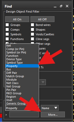
Figure 3. Rooting out obsolete properties helps ensure a clean design verification.
3. The option to find by property is selected followed by the “More…” option at the bottom right corner. That will open a list that contains all of the nets but also all of the properties which you can find at the top and bottom of the list.
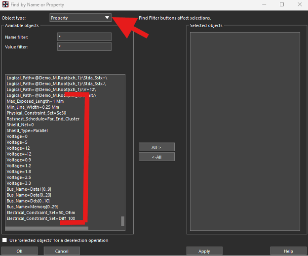
Figure 4. Once the “More” list is displayed, you can select any of the miscellaneous attributes to get a view of the affected circuits.
So, while the numerous properties address the what-if cases, the constraint manager is the preferred method for creating the guardrails wherever it applies. While there are many hooks to control line width, we have even more ways to look at the space between the traces, pads and shapes. That’s coming up next to be followed by length control.
View the next document: 03 - Controlling Air Gaps Using OrCAD X and Allegro X Tools
If you have any questions or comments about the OrCAD X platform, click on the link below.
Click here to download the PDF.