40Gb/s Since When?
The Short History of Some Marvelous Tech
Let me tell you about when 40G really meant something. A big customer (rhymes with Disco) set up a demonstration in our assembly area where they simulated the web traffic enabled by this incredible data rate. One by one they added all of the local HDTV programming, 1000 gamers, 10,000 e-mailers and so on. There weren’t as many HDTV stations in the SF Bay area back then. Even so, the refresh rates and number of scan lines made for a massive data pull for each broadcast. The point was to show us what it means to switch forty billion pulses per second - an incredible data transmission rate.
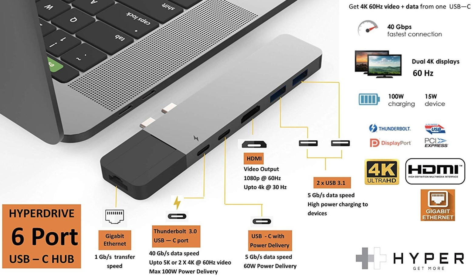
Image credit: Hyper - This Thunderbolt 3 USB hub would totally fit my blogging machine.
Who were we? An optical networking startup called Big Bear Networks that was born with the new millennium. Optical fiber could do the job of data transport over a fairly long distance. Whereas, copper wasn’t up to the job except when used with the advanced substrates of the time. This was around the turn of the century. Ceramics have been around a few millennia so we were not on to anything fancy.
At the Device Level
Low Temperature, Co-fired Ceramic (LTCC) is where the copper pattern is added to the substrate material while it is in a so-called green state. Holes are punched as needed on a layer-by-layer basis. It works out similar to the way micro vias are used on a PCB but the way they get there is quite different. It is not started from the middle; 17 layers are fine as they are simply piled up from 1 to 17.
After the additive process, the green-state clay (was never the color, green) turns to white ceramic in a kiln that bakes them - just right. The water leaving the mix has the effect of shrinking the thickness of each layer by 20%. The layers are quite thin to start with. Still, a stack of vias through too many layers will lead to a problem called posting. You get posting in the form of little slugs of metal pushing up out of the vias. When this happens on the seal-ring, you don’t get much of a seal. The way you go from top to bottom is with a series of vias that span a few layers each. That is really the major difference between an FR4 based module and a high-end package.
The 40Gb/s traces had double chamfers in the bends and the pair were exact mirror images of each other. The surrounding ground pour and vias were also perfectly symmetrical. The main drama was getting the traces under the seal ring. The first chip of the multi-chip-module (MCM) took in the 40G and spat out four pairs carrying 10G signals straight across to the second die. That die, in turn, had 16 pairs at 2.5G as its output. Those signals were the ones that went on the actual board layout.
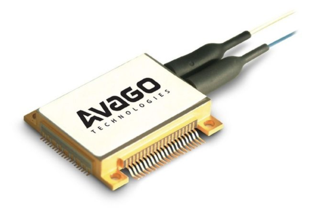
Image credit: Avago - Tiny optical transponder relative to earlier versions.
On to the Board
The form factor included a 300 pin connector. With that many pins, you have to know that it was a fine pitch affair. The only way I was able to get the 16 pairs into the connector pin-field was to stack the two traces on adjacent layers using broadside coupling rather than edge coupling. Add in the ground plane sandwich and it took four layers to route each pair of traces. Even those lines ended up being so narrow that layer-to-layer misregistration was one of our pain-points. Take two 4-mil traces on adjacent layers. If the registration is off by one mil, that represents 25% of the coupling as that portion does not overlap the positive and negative lines. Fab shops have gotten better at this because they had to.
The whole transponder was the size of a child’s shoebox. Compare this to the 10G transponder form factors that are closer to a pack of gum in size. So, guess what happens two decades later. We’re going to put 40 Gigabits per second on your desktop and, eventually, your pocket! The old shoebox has been shrunken down to the pack of gum. What an astonishing feat! It is a challenge to come up with an application that requires that much data.
Challenge Accepted
The challenge has been accepted. Augmented reality and virtual reality devices are doing some serious number crunching to simulate or enhance the real world. Robots, unmanned aerial vehicles (UAVs) and other autonomous devices are very busy with the task of sensor fusion and turning that super stream of data into immediate action. Given better hardware, the software team is always up to the challenge.
If you’ve seen a point cloud, you know what I’m talking about. We shoot lasers in every direction and turn those reflections into a real-time 360-degree view of the surroundings. It is called “simultaneous location and mapping” (SLAM). Sonar and radar also ping the environment but not at the speed of light. To keep the correction cycles to a minimum, I length-match those traces to the hilt. So, yes, automotive Ethernet is a thing.
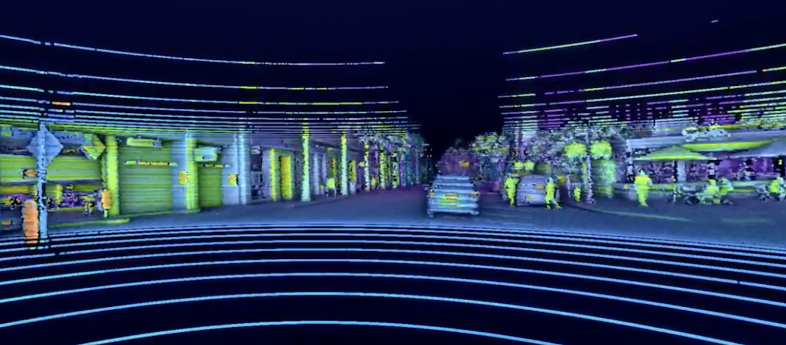
Image credit: Velodyne Lidar
Wireless technology also advances at a crisp pace. I recall a time when a start-up company announced that we had faster than Ethernet data rates with our multiple-input/multiple-output (MIMO) radios on our router chips. That type of WiFi technology is also the basis for some of the early 5th generation (5G) rollout. Huawei, Qualcomm, ZTE, and others will be battling to boast about the more capable smartphones and accompanying infrastructure.
From Tom’s Guide:
“5G is one of those heralds, along with artificial intelligence, of this coming data age,” said Steve Koenig, senior director of market research for the Consumer Technology Association. “Self-driving vehicles are emblematic of this data age, because with one single task, driving, you have massive amounts of data coming from the vehicle itself, [and] a variety of sensors are collecting a lot of information to model its environment as it moves. It’s pulling in data from other vehicles about road conditions down the lane. It could be weather information, but also connected infrastructure. There’s lots of data behind that task, which is why we need the capacity and lower latency.”
Of course, the internet backbone is shoveling data at 100 or even 400Gb/s around the server farms. Technology never stops. Network Interface Cards and cables are coming down in price and the amount of code flowing around only increases. At 40, we’re looking at a 38 pin connector with four pairs each for transmit and receive along with the usual clocks, power and ground pins. The cable itself is fiber optic so just one each for TX and RX.
With all of this new power comes new responsibility. Board design rules will continue to tighten, especially when it comes to length tuning busses and differential pairs. Loosely coupled pairs are the preferred geometry though they increase the skew when the overall path features more left or right-hand turns. Going straight or having an equal number of bends is the most elegant solution. Next up for the pairs would be dynamic phase matching where we add a little compensation bump to the trace that has the inside lane rather than simply adjusting the total length.
Digital techniques start to look like analog at these hyper data speeds. Impedance mismatches are more disruptive as the clock rate increases. A good foundation in RF is why I was headhunted into the 40G space and substrate design in the first place. All of the experienced substrate designers were captive by the companies that had the size and clout to keep their designers attached to the golden handcuffs. There are opportunities in a booming economy if you’re not averse to changes. If you’re a board designer, you live, or at least, work because of never-ending improvements. Embrace the new and it will take you to new and exciting places.