How to Measure PCB Trace Impedance with OrCAD X
Key Takeaways
-
Accurate PCB trace impedance control is crucial for signal quality and speed, preventing reflections and performance degradation in high-frequency circuits.
-
For physical boards, Time-Domain Reflectometry (TDR) or Vector Network Analyzers (VNA) methods are commonly used for trace impedance measurement.
-
OrCAD X real-time impedance analysis tools with Cross-Section Editor and Constraint Manager help enforce impedance rules and allow you to measure and optimize impedance directly in your design.
OrCAD X Real-Time Impedance Analysis
Accurately measuring PCB trace impedance will help ensure your printed circuit boards perform as expected. Understanding how to measure PCB trace impedance allows engineers to optimize their PCB designs reducing signal reflections and other impedance-related issues that can affect the reliability of high-frequency circuits. This article will explore different methods for measuring PCB trace impedance, with a special focus on how to leverage OrCAD X for impedance analysis in your design workflow.
PCB Trace Impedance Fundamentals
Impedance is the combined effect of resistance and reactance in a circuit that determines how efficiently signals travel along a PCB trace. It is defined as the opposition that the trace presents to the signal flow, which affects both the signal’s quality and its speed. Impedance mismatch can lead to signal reflections, ringing, and other distortions, which can degrade performance. In high-speed designs (e.g., USB 3.x, HDMI, Ethernet), controlled impedance is necessary to ensure proper signal transmission. The most common target impedances are 50 Ω for single-ended lines and 90 Ω or 100 Ω for differential pairs.
Methods for Measuring PCB Trace Impedance
Impedance measurement is mandatory in high-speed PCB design, RF engineering, and power distribution analysis. Various methods are available, each suited for different applications, frequency ranges, and levels of accuracy. The table below summarizes the most common physical measurement methods, which involve direct testing of circuits, components, and transmission lines.
Common Impedance Measurement Methods
|
Method |
Principle |
Frequency Range |
Applications |
Advantages |
Limitations |
|
Time-Domain Reflectometry (TDR) |
Sends a fast pulse and analyzes reflections to determine impedance variations. |
High (MHz–GHz) |
Impedance discontinuity detection. Industry standard for PCB & cable testing. |
Fast, non-destructive, high-resolution measurements. |
Expensive, and requires expertise to interpret results. |
|
Vector Network Analyzer (VNA) |
Measures S-parameters to determine impedance across frequency. |
Wideband (kHz–GHz) |
PCB trace impedance. Industry standard for RF/Microwave. |
High accuracy, suitable for RF/microwave applications. |
Expensive, and requires expertise to interpret results. |
|
Impedance Analyzer |
Applies an AC signal and analyzes voltage and current response. |
Low to High (Hz–GHz) |
Power distribution networks (PDN) analysis and passive components testing. |
Direct impedance measurement and is highly accurate. |
Limited to lab environments, and may not be suitable for in-field testing. |
|
LCR Meter |
Measures impedance at low/mid frequencies using bridge circuits. |
Low to Mid (Hz–MHz) |
Capacitor, inductor, and resistor characterization, passive component testing. |
Simple and cost-effective, widely used. |
Not suitable for high-frequency applications. |
|
Field Solver (Sigrity X) |
Uses numerical methods to simulate impedance based on PCB stack-up, trace geometry, and material properties. |
Simulation-Based |
Industry standard for pre-layout design and material modeling. |
No physical testing is required, useful for early design stages. |
Accuracy depends on model assumptions and requires computational resources. |
Measure PCB Trace Impedance with Time-Domain Reflectometry (TDR)
The most common method to measure PCB trace impedance for a physical board is Time-Domain Reflectometry (TDR). TDR works by sending a fast signal pulse down the trace and measuring the reflections that occur when the impedance changes. These reflections indicate the points along the trace where impedance mismatches occur, allowing you to pinpoint areas that need correction. A TDR setup typically includes:
-
Pulse Generator: Sends a fast pulse down the test trace.
-
Oscilloscope: Measures reflections and displays them on a screen.
-
Reflection Analysis: The amplitude of the reflected pulse is analyzed to determine the impedance at various points along the trace.
The rise time of the test pulse used by the TDR must match the rise time of the signal in the actual circuit. If the rise times differ significantly, the impedance measurements could be inaccurate.
How To Measure PCB Trace Impedance In OrCAD X
If you’re wondering how to measure PCB trace impedance in OrCAD X, look no further than the integrated tools for impedance analysis that provide designers with capabilities for analyzing trace impedance directly in the design environment.
Cross-Section Editor and Constraint Manager
-
Cross-Section Editor: This tool allows you to define the stackup of your PCB and calculate impedance based on trace width, height, and material properties. You can adjust parameters such as trace width and dielectric thickness to meet your target impedance, ensuring that the impedance is consistent across all layers of the PCB.
-
Constraint Manager: The Constraint Manager will enforce impedance rules during the design process. It allows you to define impedance requirements (e.g., 50 Ω) for different layers and nets. As you route traces, OrCAD provides real-time feedback, ensuring that the impedance remains within the desired range.
Real-Time Impedance Analysis
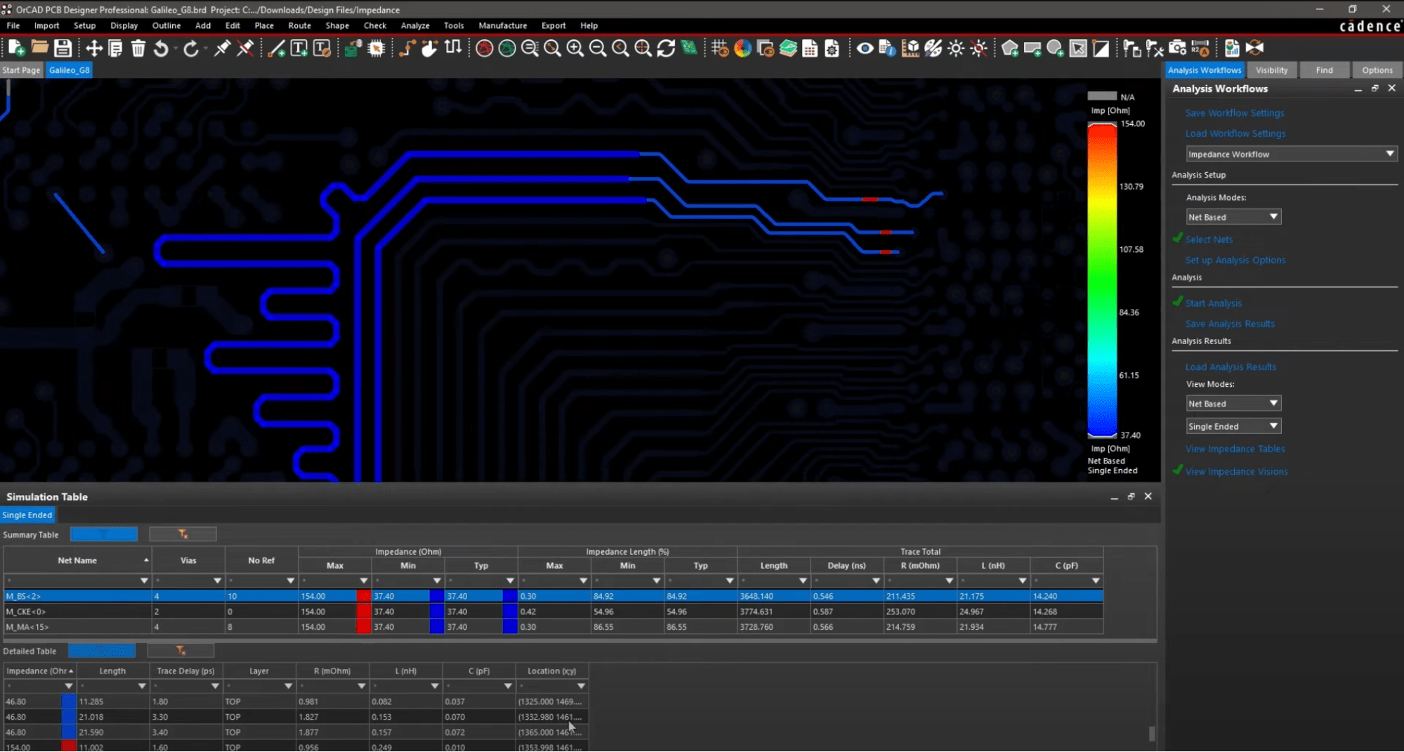
Real-Time Impedance Analysis Workflow in OrCAD X
The integrated impedance analysis workflows in OrCAD X, powered by Sigrity X Aurora, allow you to easily identify and resolve real signal integrity problems in your design.
-
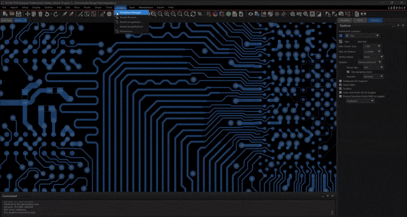
Click Analyze → Workflow Manager
-
Click Select Nets then Filter and select the critical nets in your design, and click OK.
-
Start Analysis
-
Select View Impedance Visions to see a color-coded scale from red to blue showing which traces in your design have the highest impedance.
-
Select View Impedance Tables to see your traces with impedance in a table. Quickly navigate to the problem area by clicking on a data point from the table, and you'll jump directly to that trace.
-
Adjust to fix the issue and run the analysis again to see the results
Learn how to measure PCB trace impedance with OrCAD X to ensure optimal signal integrity and high-speed performance. Set and enforce impedance constraints directly in your design with the Constraint Manager and real-time impedance analysis. Explore how Cadence’s OrCAD X platform can streamline your impedance measurement process and try a free trial today.
Leading electronics providers rely on Cadence products to optimize power, space, and energy needs for a wide variety of market applications. To learn more about our innovative solutions, subscribe to our newsletter or our YouTube channel.