How to Measure Bow and Twist on a PCB: Techniques and Tools
Key Takeaways
-
Bow and twist in PCBs are measured using specific IPC standards. Bow is assessed by the maximum distance from a flat surface to the highest point, and twist is assessed by the height difference at one corner while others remain flat.
-
According to IPC-6012 standards, bow and twist should not exceed 0.75% for PCBs with surface-mounted components.
-
To reduce the risk of bow and twist, evenly distribute copper across your PCB. Regions with high and low copper density may lead to internal dresses causing bow or twist.
How to measure PCB bow as a percentage
PCBs ideally need to be completely flat, but achieving this is often challenging. Warping, known as bow and twist, typically happens during and after the PCB production process. A PCB bow describes a curvature where the board bends into a convex or concave shape along its length or width. On the other hand, a PCB twist involves the board warping in a rotational manner around its center, resulting in its corners being uneven and not lying on the same plane. Read on as we explain how to measure bow and twist on PCBs.
Contributing Factors to PCB Bow and Twist
- The presence of large copper planes or traces concentrated in specific areas
- Asymmetrical layer arrangements with varying thicknesses
- Board pressing parameters
- Material selection
- Component placement
How to Measure Bow and Twist on a PCB
According to IPC TM 650, bow and twist in PCBs are measured differently. According to IPC6012, the maximum bow and twist for boards with SMD components is less than 0.75% and 1.5% for those without.
- A bowed PCB has all four corners touching a reference plane, and its deflection is measured from the highest point off the table. The bow calculation considers the deflection relative to the board's length or width.
- A twisted PCB does not have all four corners touching the reference plane; there is a deflection along the diagonal. One method to measure this involves restraining three corners and allowing the fourth to rise freely, then measuring the deflection at the raised corner.
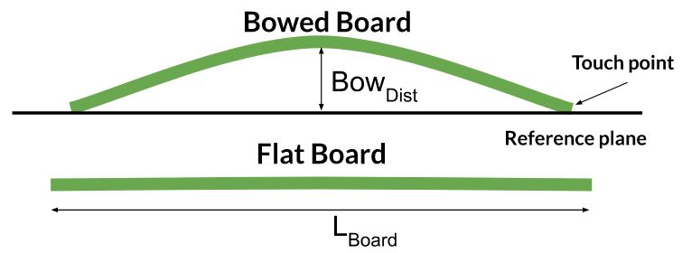
How to Measure Bow on a PCB
Based on the procedure from IPC-TM-650, bow can be measured with the following equation.
PCB Bow Measurement
Bow% = (BowDist / LBoard)* 100%
Where:
-
Bow% is the percent bow of the board, and should be kept less than 0.75% if with SMD components.
-
LBoard is the length of the board flat. This can be measured through your EDA software.
-
BowDist is the maximum bow distance — when placed on a flat surface, it is the distance from the surface to the highest bowed point on the board, as shown in the first diagram.
How to measure PCB twist as a percentage
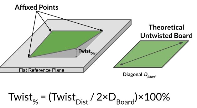
How to Measure Twist on a PCB
A PCB has twist if, when laid on a flat reference surface, two or three corners of the board remain touching the flat surface. To measure twist, affix the third corner to the reference plane such that only one corner of the board is raised as shown in the diagram. Then, measure the twist distance.
PCB twist can be measured using the following equation.
PCB Twist Measurement
Twist% = (TwistDist / 2×DBoard)×100%
Where:
-
Twist% is the percent twist of the board and should be kept less than 0.75% if with SMD components
-
DBoard is the diagonal length of the theoretical flat board, specifically the diagonal with two corners that lay flat.. This can be measured through your EDA software.
-
TwistDist is the maximum twist distance — when placed on a flat surface, it is the distance from the surface to the highest twisted point on the board, as shown in the diagram.
To ensure the accuracy of this method, three of the board's four corners must make contact with the reference plane, with only one corner being physically pressed. If this setup is not feasible, the IPC-TM-650 outlines a more intricate 'referee method' that can be employed.
The Consequences of Not Measuring Bow and Twist
Warping and bowing can result in misalignment during assembly, complicating the precise placement and securing of components into the board's holes and pads. Moreover, these deformations can cause problems with signal integrity, induce mechanical stress, degrade performance, and eventually lead to component failure over time.
Measuring Bow and Twist With OrCAD X
To reduce the risk of bow and twist, it is crucial to meticulously plan the layer stack-up design and copper distribution, handle and store PCBs properly during and after manufacturing, and select PCB materials with low thermal expansion coefficients. These measures help maintain the flatness and stability of PCBs throughout their lifespan.
In order to minimize bow and twist on your PCB, it’s important to distribute copper as evenly as possible throughout the board, thus minimizing internal stresses. OrCAD X has a variety of tools that you can use to do this.
OrCAD X Tools to For Managing Copper Distribution
|
Section |
Description |
OrCAD X Tools |
|
The cross-section editor allows you to set up and adjust the stack-up. You can add or remove layers, set thickness, material, and surface finish for each layer. |
|
|
|
Managing Copper Shapes |
Copper shapes can be managed using tools to create, merge, and assign nets to shapes. Shapes can be created as rectangles or polygons and merged if needed. The Z Copy method can be used to copy shapes to other layers or with an offset. |
|
Now that you understand how to measure bow and twist on a PCB, enhance your future designs with OrCAD X. Experience these features firsthand—sign up for a free trial of OrCAD X today!
Leading electronics providers rely on Cadence products to optimize power, space, and energy needs for a wide variety of market applications. To learn more about our innovative solutions, talk to our team of experts or subscribe to our YouTube channel.