Common PCB Failure Reasons and How OrCAD X Minimizes Them
Key Takeaways
- Component failures, faulty traces, power issues, design errors, and environmental factors can all lead to PCB failures.
- Advanced features like Live BOM, real-time DRCs, signal integrity analysis, and DFM checks help minimize potential failure points in PCB design.
- OrCAD X addresses manufacturing-related issues such as plating voids, copper-to-edge clearance, and bad soldering to ensure high-quality PCB production.
There are numerous PCB failure reasons, from power failures to component failures.
Printed Circuit Boards (PCBs) appear in virtually every electronic device. At the same time, it seems they may break due to a variety of PCB failure reasons. Below, we’ll take a look at some common PCB failure reasons and how advanced software tools like OrCAD X can help identify or minimize potential failure points in the design phase, reducing costs associated and creating more reliable PCBs.
Major PCB Failure Reasons Summarized
|
Cause |
Description |
|
Component Failures |
|
|
Faulty Traces |
|
|
Power Failures |
|
|
Design Errors |
|
|
Plating Voids |
|
|
Insufficient Copper-to-Edge Clearance |
|
|
Bad Soldering |
|
|
Slivers |
|
|
Acid Traps |
|
|
Thermal Issues |
|
|
Electromagnetic Issues |
|
|
Environmental Factors |
|
|
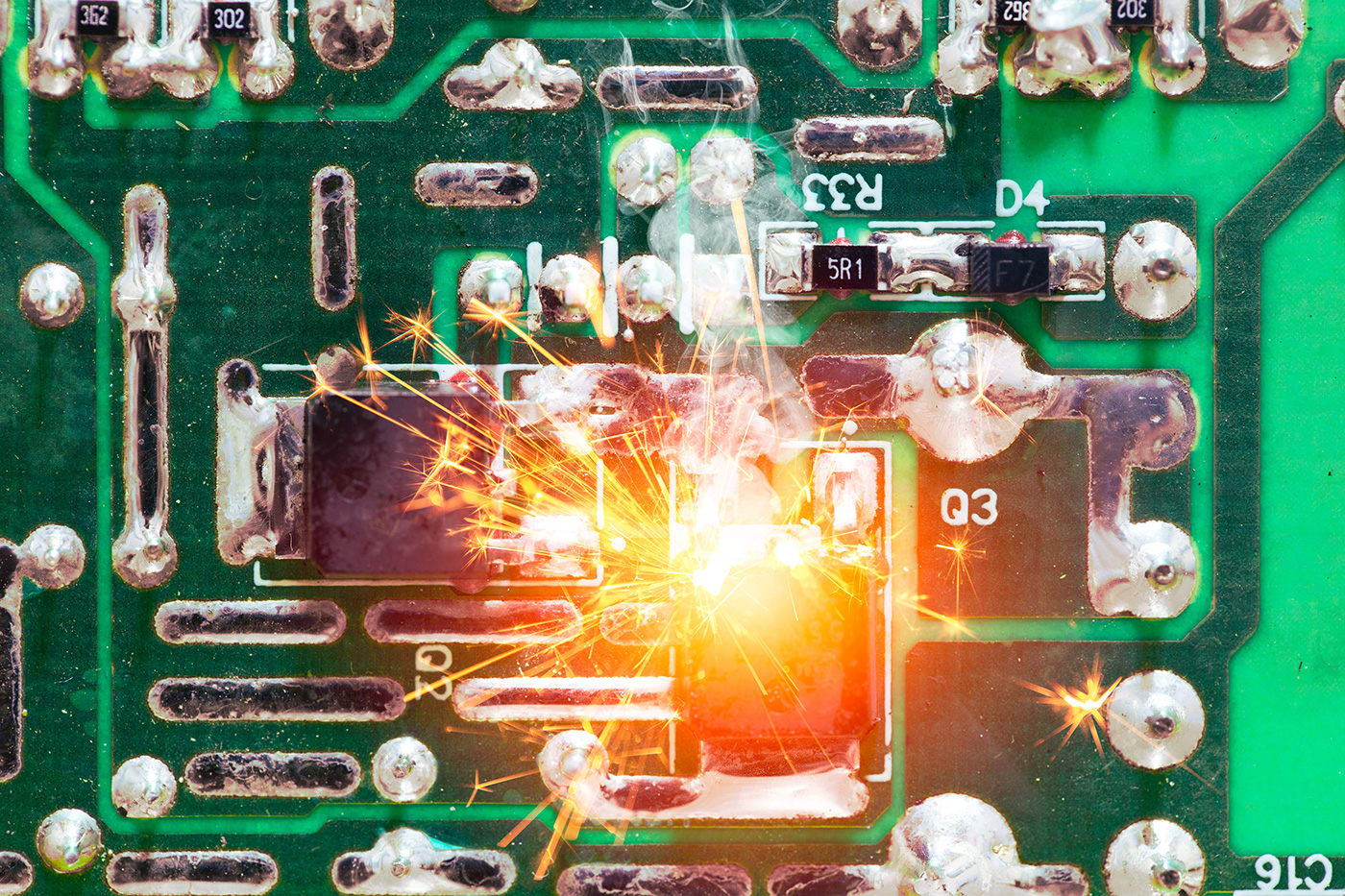
Burned Circuit Boards |
|
|
Age |
|
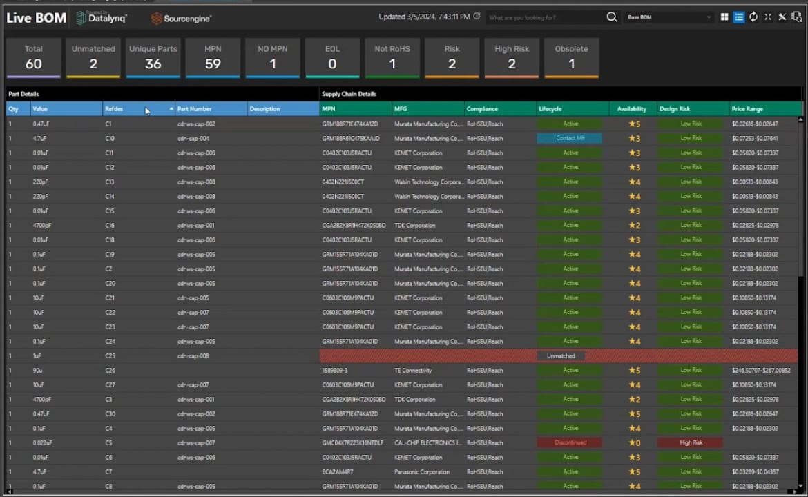
OrCAD X Live BOM provides compliance lifecycle, status, market availability, and price.
Component Failures
OrCAD X reduces the risk of component failures through its advanced Live BOM and component sourcing capabilities. The Live BOM feature, integrated with Sourcengine, provides real-time visibility into the lifecycle, compliance, and market availability of components, ensuring that only high-quality, reliable parts are used.
Designers can view detailed information about each component, including manufacturer part numbers, compliance data, and risk scores. This comprehensive data helps them select components that meet the required standards, reducing the risk of failure due to poor quality or incorrect specifications.
The tool provides alternate part suggestions for high-risk components, ensuring that substitutes are readily available, thereby maintaining the integrity and reliability of the design.
Faulty Traces
OrCAD X helps prevent faulty traces through real-time Design Rule Checks (DRCs). The platform's constraint-driven routing ensures that traces are designed with adequate width and spacing, reducing the risk of overheating and breakage. The integrated DRCs continuously monitor the design, highlighting potential issues such as inadequate trace width or spacing.
Power Failures
OrCAD X in conjunction with a Sigrity X Aurora license, enables the use of advanced power integrity analysis tools to detect and prevent power failures. The platform offers power-aware routing and power distribution network (PDN) analysis, ensuring that the voltage supply is adequate and correctly distributed across the PCB. By simulating the power network, designers can identify and resolve issues such as inadequate voltage supply and incorrect loading
Design Errors
OrCAD X minimizes design errors through its integrated schematic capture and layout environment. The platform provides real-time feedback and constraints management, allowing designers to catch and correct errors during the design phase. Features such as automated layout suggestions and constraint-driven design ensure correct component placement, adequate spacing, and accurate schematic entry.
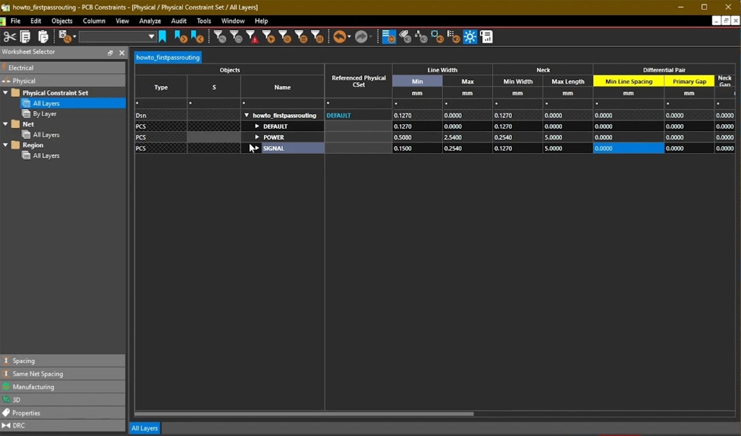
Constraint manager in OrCAD X ensures physical constraints are adhered to. In the case of this image: power and signal trace widths.
Plating Voids
Design for Fabrication (DFF) checks can identify and prevent plating voids. OrCAD X includes specific checks for the manufacturing process, ensuring that plated through-holes are correctly formed and free from contamination or air bubbles.
Copper-to-Edge Clearance
Constraint management tools ensure sufficient copper-to-edge clearance by setting specific design rules. Designers can define clearance constraints for the copper layer, preventing it from being trimmed too close to the edge during manufacturing with real-time DRCs enforcing these rules.
Starved Thermals and Burned Boards
OrCAD X thermal management features can identify and prevent starved thermals. The platform offers detailed thermal analysis with Celsius Thermal Solver, ensuring that heat dissipation is adequate and voids are minimized.
Manufacturing-Related Failure Reasons
OrCAD X effectively addresses critical manufacturing and assembly issues such as acid traps, slivers, and bad soldering, through Design for Manufacturing (DFM) checks. These checks prevent acid traps by optimizing circuit angles to avoid excessive corrosion during the etching process. By providing real-time feedback and automated rule checks, designers can adjust the layout to eliminate these issues before production. Additionally, OrCAD X Design for Assembly (DFA) checks aid in creating defect-free reliable solder joints.
Understanding the common PCB failure reasons is crucial for designing reliable and high-performance PCBs. To explore how Cadence's suite of PCB design tools can enhance your design process, visit our PCB Design and Analysis Software page. Learn more about the powerful capabilities of OrCAD X to ensure your PCBs designs are perfected.
Leading electronics providers rely on Cadence products to optimize power, space, and energy needs for a wide variety of market applications. To learn more about our innovative solutions, talk to our team of experts or subscribe to our YouTube channel.