PCB Edge Connector Design With OrCAD X
Key Takeaways
- PCB edge connectors are the premier system integration method for high-speed data transfer and modular assemblies.
- Proper mating between the board edge and connector requires a chamfering process to protect the connector pins.
- The selection of edge connectors will boil down to the assembly and fabrication constraints of the joined boards.
PCB edge connector design allows for high data throughput with multiple parallel lines.
System integration comes in many shapes and sizes: connectors can vary wildly depending on the manufacturing needs of the board, and none stand out (literally and figuratively) as much as PCB edge connectors. Instead of using interfacing equipment like cables or flex circuits, edge connectors allow PCBs to plug directly into the receptacle for a board-to-board connection style. While this arrangement is less suitable for densely integrated systems or tight enclosure form factors, PCB edge connector design is an excellent choice for high-speed data throughput and repeated insertion/removal cycles.
Comparing Different System Integration Methods
|
Board-to-board |
Board-to-wire |
Wire-to-wire |
|
|
|
Considerations for PCB Edge Connector Design
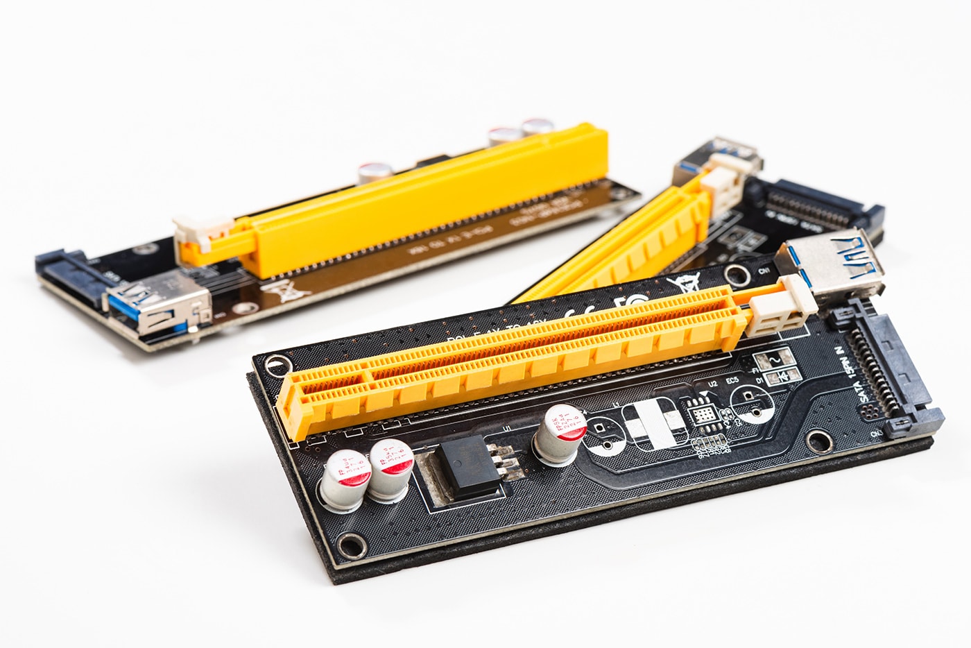
PCB edge connectors use copper placed at the edge of the boards (while still adhering to edge clearance rules) to support the direct integration of secondary boards into the primary board. The most well-known application of PCB edge connectors is the expansion cards found in desktops for expansion and video game cartridges before the rise of compact disk media in the mid-90s. A few advantages of a PCB edge connector are that the format only requires a receptacle as the board forms the plug. To achieve this, the daughter board requires chamfering on the leading edge to guide the PCB into the socket and lock it in place; most often, chamfering occurs at a 30° angle on either side of the board, but wider and narrower cuts are possible (note that broader cuts reduce the board edge clearance constraint). Additionally, while standard chamfering operations are constrained to an outer edge of the board, more advanced chamfering options include placement inside of leading edges or border contours, but this depends on the exact capabilities of the manufacturer.
As the designer, it’s your job to ensure your board can easily mate with the standard edge connector on the mating board. That’s where chamfering comes in—you need to ensure that the mating edge of your PCB meets the chamfer angle and tolerances specified by the edge connector manufacturer. You’ll also want to ensure the fabrication house you choose meets the tolerances and chamfer angle you desire. To give you an idea, here are some standard design parameters you’ll encounter for PC and PCI cards:
- Chamfer angle: 45° for PC, 20° for PCI
- Chamfer depth: 0.5 mm for PC and PCI
- Gold finger spacing: 0.7mm for PC, 2.0mm for PCI
Chamfering complements the connector design, with pins rising at a shallow angle from the vertical towards the mating board. While the width of the connector ensures a tight fit, the angled pins maximize contact with the chamfered angle and minimize the vertical pull force on pins during card edge removal. Mechanically, edge connectors provide robust connectivity with many insertion/removal cycles before failure. The connector alone is a more straightforward setup than a board-to-wire connection as it features fewer points of failure, and no additional resistance arises from the connection (i.e., the total resistance is the contact resistance between the edge connector and pins).
Design Factors That Can Impact Edge Connector Performance
Relative to standard plug/receptacle connectors, the construction of PCB edge connectors makes them extremely durable and highly reliable, and they are ready-made for multi-board assemblies. However, there are a few constraints to keep in mind:
- Board thickness - Because the connector builds around the width of an entire PCB, extraordinarily thick or thin boards are incompatible with standard connector design. Fortunately, standard board thicknesses of 1.6 mm/63 mils are acceptable, and there is still considerable leeway for the allowed thickness (in either direction) that supports multiple design configurations.
- Mounting - Due to the high forces associated with multiple insertion/removal cycles, connectors require extra mechanical features that provide support and relief across the service life of the connector. Typically, this can come in the form of weld tabs that solder as part of standard manufacturing processes but provide no electrical functionality or through-hole pins and matching drilled holes that keep the connector in place. The standard differences between surface mount and through-hole implementations apply, namely that the former is more conducive to HDI designs and can be cheaper if it’s part of automated assembly; however, the size of edge connectors may require manual assembly and soldering that can add nontrivial costs lot sizes of even moderate volume.
- Backplane intricacy - A board may be a general design incorporating one or more edge connectors alongside other circuitry or an explicit backplane exclusively designed around edge connector integration. The latter’s purpose hinges on reliability: with fewer active elements (or none at all) on the board, there is little chance that card swapping or routine maintenance causes damage to the board. In other words, all or nearly all of the circuitry is on the daughter card. While it can be advantageous, this method severely restricts the design, and active elements on the board that contain a layer of redundancy are usually a better option.
Cadence Has Cutting-Edge Solutions for PCB Design
PCB edge connector design is a unique connector format that supports repeated insertion/removal cycles instead of a single, permanent assembly configuration. These edge cards offer great performance for high-speed operations, although space considerations are sizable compared to board-to-wire or wire-to-wire connections. Designers must be aware of the DFM aspects of edge connectors; Cadence’s PCB Design and Analysis Software suite provides all of the necessary tools for constraint-driven applications. Alongside the fast and powerful OrCAD X Presto PCB Editor, ECAD has never been easier or more modular.
Leading electronics providers rely on Cadence products to optimize power, space, and energy needs for a wide variety of market applications. To learn more about our innovative solutions, talk to our team of experts or subscribe to our YouTube channel.