The Implementation of Design Reliability Testing and Risk Reduction Strategies
Life is full of lessons, and some of them are easy to see, learn, and put into action, whereas others require a bit of a learning curve. However, my favorite life lessons are those passed down from years of wisdom.
I recall one lesson, in particular, taught to me by my grandparents in regards to reliability, risk reduction, and the care of my items in general. “You will never have all that you desire to own if you keep having to buy the same things over and over before there is a need.”
The lesson itself is rather straightforward, so long as you understand that this life lesson is multifaceted. The first bit of wisdom I gleaned from this lesson is: take care of my items and limit the risk of damage, i.e., risk reduction. The second facet is equally apparent, and it pertains to the reliability phase of all things. If you take care and reduce the risk of damage, the inherent reliability of an item will reach its maximum potential. This same life lesson is adaptable to the world of electronics and PCB design, especially since reliability is a cornerstone of proper PCB design.
Why is Design Reliability Testing Needed for PCBs?
As a fundamental rule, one should design and build your PCB with reliability in mind. Regardless of the end product, the service your company provides, or how many new customers you obtain, it is the repeat customers that promote longevity in any business. The best way to retain customers is through excellent customer service and of course, the reliability of your product or service.
When we consider the world of PCB design, there are guidelines and standards that must be followed to achieve an optimal and accurate design. Even then, there must be testing and design testing (simulation) to ensure that the product performs as intended and is reliable over a specified length of time. These tests are essential in assessing PCB performance, reliability, and accuracy of the designs. As I am sure you are aware, the one thing no PCB designer wants is, discovering at the last minute that their product fails or is faulty.
As mentioned earlier, even properly designed and pedantically built PCBs, are susceptible to faults and failures. Most electronic devices come out of the prototype phase with issues that require PCB designers to troubleshoot further. However, it is those problems that escape notice until the product is in the field that are the most upsetting for a company or business. These warrant the need for electronics testing, a need that is exponentially greater for PCBs because they are in use in practically every electronic device.
What is Tested to Ensure PCB Reliability
It is common knowledge among engineers that PCB testing is a vital part of the development and design process for PCBs. Conducting these tests from the beginning of the design and lasts through the production process helps to reduce costs and derail issues before they become a significant problem in the end product. Furthermore, there is a wide array of PCB testing methods that are in use on physical (PCB) boards. Many of which you can implement on small-scale assemblies or prototypes.
Reliability testing starts from the schematic and hardware design itself. It is conducted on the basis of component properties and the way they are placed in circuit design. These tests aim to look more closely at potential solder joint issues, shorts, and issues with functionality. All of these checklist items increase PCB reliability and improves overall design and functionality, ensuring that each tested PCB will function as intended. These types of tests also offer other benefits in the PCB design process such as;
Saves time: Reliability type tests save time because it points out the areas that need improvement quicker. This, in turn, makes it easier for designers to address the problems quickly and efficiently. Overall, it increases productivity, reduces risk, increases reliability, and reduces cost.
Finds errors: The goal of all PCB designs is a high level of functionality, performance, and the ability to do so over the life-cycle of the end product. That is why finding bugs and errors as soon as possible, garner a higher level of reliability and reduces the risk of reliability issues in the future.
Reduces cost: Due to the discovery of errors, faults, and possible reliability issues early on, it saves a company money and reduces the risk of reliability issues in the future.
Although not all types of PCBs require the same amount of rigorous testing, they do generally have the same items or areas tested. These items or areas are as follows:
Lamination: Especially since lamination quality is critical to the lifespan of a PCB. Furthermore, peeling laminate can cause issues in the final functionality of a PCB.
Copper plating: These are tests for copper quality, i.e., tensile strength, and elongation.
Solderability: Assures that components can be securely attached to the PCB. This test is also a focus on wetting or the ability of the surface to accept liquid solder.
Hole wall quality: Test to ensure that the hole wall will not crack or delaminate. The emphasis of the test is to subject the PCB to environmental stressors to ensure reliability.
Electrical: Tests the ability of the PCB to conduct electrical signals with minimal leakage.
Environment: Tests the reliability of a PCB to resist water absorption in a humid environment.
Cleanliness: Tests the ability of a PCB to resist environmental factors such as humidity, corrosion, and other environmental conditions.
Types of Testing Methods for PCB
There are numerous PCB testing methods that one can utilize, but no single test will detect every issue or adhere to every requirement a designer might have. Therefore, you should consider these testing methods carefully to ascertain which of them meets your specific needs. Also, there are some factors one should consider before arriving at a decision on which method best suits your needs. They include the reliability of the testing method, the issues you are testing for, and the type of product you are testing.
Overview and Summary of Testing Methods
In-Circuit Test (ICT)
It allows a manufacturer to test the individual components as well as to measure their performance, regardless of the other parts attached to them. Also, it is capable of detecting 98 percent of faults and is best for analog circuits since it excels at measuring capacitance, resistance, and other analog measurements.
Fixtureless In-Circuit Test (FICT)/Flying Probe Test
FICT is a type of ICT that operates without the need for a custom fixture, thus reducing the overall cost of the test. Instead, it uses a simple fixture to hold the board while test pins move around and test relevant points on it using a software-controlled program, hence the name flying probe test. Although it is an efficient and cost-effective testing method, it tends to be slower than the standard ICT.
Functional Circuit Test
A functional circuit test (FCT), as its name implies, is a test that tests circuit functionality. FCTs simulate operational environments consisting of any potential device that may communicate with the device under test (DUT), and simulate the final electrical environment that the device may use. These types of tests may vary, but they all simulate the operational environment of the PCB in question.
Boundary Scan Testing
The boundary scan test examines the traces of a PCB. It provides a method of testing integrated circuits when it is not possible to reach all the nodes of a circuit. It is generally in use in field service to find issues within functioning systems.
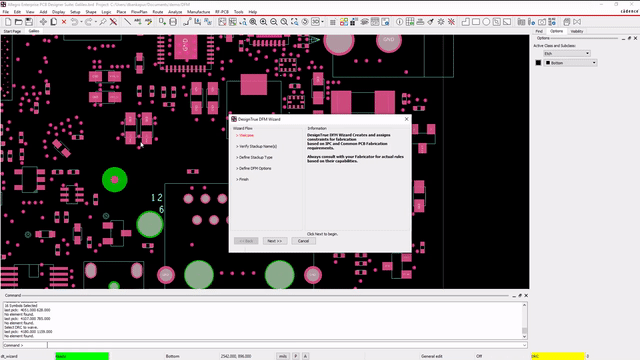
Design for Manufacturing (DFM) Testing
Design for Manufacturing (DFM) is the process of assembling a PCB topology with a focus on the manufacturing method. This is a design mentality that focuses on mitigating issues that generally occur during the fabrication and assembly process. In general, you should implement DFM testing early in a project timeline to reduce the overall development time and costs.
Design for Assembly (DFA) Testing
For PCBs, assembly is as important as the design itself. Therefore, testing the Design for Assembly (DFA) is equally essential. Regardless of the components in use, you need to be able to securely and effectively assemble them to achieve the final product. Also, you should implement DFA testing as early in the design process as possible to minimize production costs and reduce development time.
Design for Test (DFT)
Design for test (DFT), as its name implies, refers to a PCB’s design that makes it easier to test. All PCBs require some degree of testing; therefore, it is prudent that your design accommodates this in an efficient manner. With such an emphasis on testing, it stands to reason that testing to ensure this is possible, incorporates a high degree of importance.
Note: Although DFT requires additional design and engineering in its implementation, it pays dividends with a reduction of faults and manufacturing costs.
Design for Supply Chain (DSC)
DSC is a focus on the life cycle of a product. In general, it points to the use of components in the design that are easier to source and are also cost-effective. This makes the end product easier to manufacture and repair if needed. So, testing DSC is also an important aspect to consider, and it has a direct effect on reliability. For example, if you purchase a new OLED 4K TV and after 6-months (12-month warranty) of use it needs repair, but the required components for said repair costs more than the initial purchase; well you get the idea.
Situations like this would be a nightmare for companies doing the warranty work and for the consumer as well if this were to happen outside of the warranty period.
Ensuring there is adequate testing in place for a design is helpful before production.
IPC and the Class Standards Set for PCB Classification
IPC is an organization that produces PCB-related standards. The association was formerly called the Institute for Printed Circuits but is presently called the Association Connecting Electronics Industries. IPC standards are the electronics-industry-adopted standards for design, PCB manufacturing, and electronic assembly.
Within the IPC’s standards are the dividing classes that categorizes PCBs. They are as follows:
Class 1 Electronics: It consists of General Electronics Products, such as toys, flashlights, and smartphones. Overall, these are electronics products that have a short life cycle and have the lowest standard of quality or reliability.
Class 2 Electronics: It includes Dedicated Service Electronics Products, such as laptops, microwaves, and televisions. Overall, these devices have a long or extended life cycle, where continued performance is required or expected. In other words, devices that promote uninterrupted service, but it is not critical.
Class 3 Electronics: Class 3 electronics encompass High-Reliability Electronics Products, such as aerospace, military, and medical applications. These devices have a very long life-cycle with the highest level of standards. They promote failsafe performance and functionality as well as uninterrupted service. The devices within this class offer functionality that is critical and is subject to the strictest guidelines.
A fully-functioning as-intended printed circuit board is ideal in every design.
Designs that promote reliability is the ultimate goal of every PCB designer. The standards set by the IPC offers a blueprint on how and why reliability is so important. Although we may never experience firsthand why PCB reliability is so essential, however, one visit to a critical care floor of a hospital would put this into perspective. Reliability goes beyond profit margins and returns on investments, because sometimes about life and death.
With Cadence’s suite of design and analysis tools, you’ll be sure to have your designers and production teams working together towards implementing design reliability and risk reduction strategies to optimize all of your PCB designs. Allegro PCB Designer is the layout solution you’ve been looking for, and it can unquestionably facilitate the implementation of design reliability and risk reduction strategies into your current and future PCB designs.
If you’re looking to learn more about how Cadence has the solution for you, talk to us and our team of experts.