Electronic Interconnect Design Considerations in PCB Layout
A few years ago someone asked me for some advice on a problem they were having with their recreational vehicle (RV). At first I wondered why they were asking me, but then I realized that I have actually been doing this for well over 20 years and I have more experience on the subject than I thought. I have specialized tools and devices that I use for specific RV needs, and I have a set pattern of hooking up, towing, and parking my trailer with my truck. After a while you learn how to do things a certain way for the best results.
It is no different with PCB layout. After many years of designing boards, there are several electronic interconnect design considerations that I have picked up as well. These include how I work with component placement, set up for my routing, and creating my output files. If you haven’t had much experience with PCB layout yet, perhaps some of these details may be of help to you.
Electronic Interconnect Design Considerations for Component Placement
The best way to start your layout is to make sure that you are prepared with as much information and data up front as possible. Start by asking yourself some of these questions:
- Do I have complete and accurate library data?
- Do I have up-to-date mechanical information for my board features and dimensions?
- Do I have enough data to correctly configure my board layer stackup?
- Do I have all the necessary information on sensitive part placement for high speed circuitry and thermal issues?
- Do I have all the specifications on high speed routing requirements?
These are the “big ticket items” to ask about, but there can be a lot more depending on the specific needs of your design. The important thing is to be prepared.
To start component placement it is often helpful to group your parts around the exterior of the board according to their schematic circuitry. Using the schematic you can easily find and select grouped components in order to maneuver them around in layout.
One of the advantages of doing this before you start placing the parts within the board outline is that you can see everything that you will be working with. With all the parts organized like this, it is easier to see where groups of components need to be placed according to any high speed, thermal, or mechanical requirements that they might have.
Now that you’ve got a good start on your component placement, let’s take a look at some of the specifics about routing that you should consider.
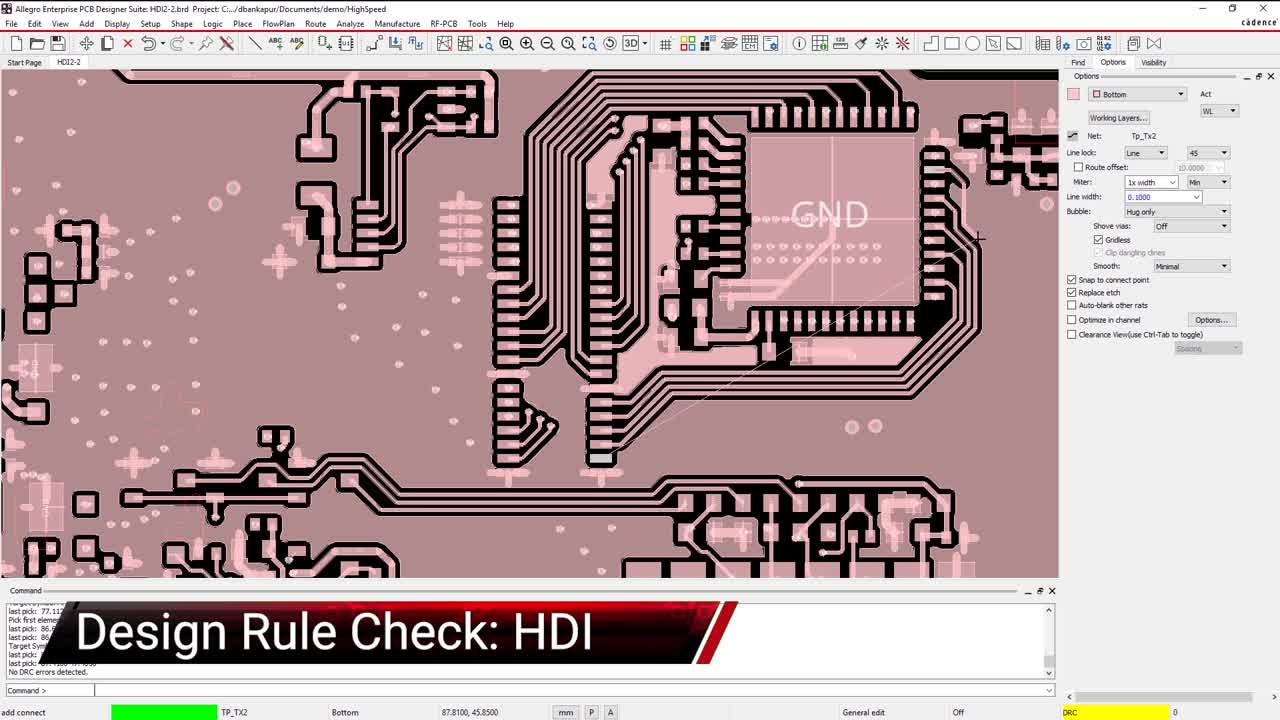
Using constraints makes trace routing a much easier task
Some Key Considerations for Routing Your PCB Layout
The first and best thing that you can do to help you succeed with your routing is to fully set up your design rules. Here are some of the key rules and constraints that will have the biggest influence over your routing:
-
Nets: You will want to set up width and spacing trace routing constraints for routing and specific constraints for nets such as power & ground. We prefer defining planes for such nets.
-
Net Types: These rules will enable you to apply specific constraints to multiple nets for example, imposing restraints on routing layers, on-via types, and enabled trace-widths.
-
Differential Pairs: Your layout tools will have specific routing features that will allow the two nets of a differential pair to be routed in tandem. You can set up rules and constraints for these pairs in the same way that you do nets and net types.
-
Measured Trace Lengths: Some nets may require that they be routed to a certain length. Your layout tools will be able to assign those lengths to the nets as a constraint.
-
Vias: The vias that you use can have many different rules assigned to them. Rules for different sizes, which layers they can span, and which nets they are used for.
-
Misc Objects: You can also create rules like clearance and creepage distance between various conductive elements of pcb, how close you can get to holes, pads, vias, keepout zones, and many other PCB objects as well.
There are many other rules and constraints that can be set up including matching trace lengths, routing topologies, and signal paths. The important thing is to set up as much as you can to help yourself while you work. I have seen many PCB layout designers who do not fully utilize their design rules and constraints. Although they can get a jump on their routing, they are also forced to rely on their memory to meet specific routing tolerances and do a lot of extra cleanup work to fix their errors.
It is also good to get into the habit of planning out your routing patterns while you are placing components and determine which board layers will be used for those patterns. You also need to allow enough space for all the routing as well as any sensitive nets that may require additional widths and spacing. The last thing anyone wants is to have to rip up and replace a lot of component placement and routing in order to squeeze in the last few traces. And finally, be careful about routing traces across split planes. These could cause serious problems with the return paths of the nets and degrade the signal performance of the PCB.
Now that the board is placed and routed, it’s time to get it built. Here again it is important to consider carefully what you are doing so that you can send out accurate data to your manufacturer.
A full set of design rules will allow you to set up a wide range of routing constraints
Don’t Ruin Your Design with Careless Manufacturing Documentation
All too often PCB layouts have problems being manufactured because there wasn’t enough care and attention spent creating the final documentation. Unfortunately manufacturing documentation is often viewed as “busywork” by some layout designers instead of getting the full attention it deserves. As a result the manufacturer either delays the build until they clarify the documentation, or end up with a bad board build.
Make sure that you create your manufacturing documentation as accurately as possible, and take a moment to review the material that you create. If something in it isn’t clear to you, then you can bet that it won’t be clear to the manufacturer as well. Drawings need to clearly communicate build instructions and reports need to have precise data and information in them.
Another important electronic interconnect design consideration is what PCB design tools should you use. Allegro PCB Designer has the constraint driven design process that we’ve talked about here, as well as a host of other productivity enhancements that will help your layout all the way from placement to your final manufacturing documentation.
If you’re looking to learn more about how Cadence has the solution for you, talk to us and our team of experts.