Functional Partitioning in PCB Design
Key Takeaways
-
Why you need functional partitioning in PCB designs.
-
Considerations when setting up functional partitions.
-
Leveraging the features and capabilities of the PCB design tools for partition creation.
They may be known as frozen microwave meals today, but when I was a kid, we knew them as TV dinners. These delights came in crinkly aluminum trays that were partitioned into separate sections all covered with foil, ready for the oven. And, if you were really lucky, the food under the foil might even remotely taste like the dishes pictured on the box. The key to their success, however, was the partitions in the trays which were designed to keep the food separated both for packaging and cooking.
This same principle of partitioning is also used in the design of printed circuit boards, where there are different groups of circuits that perform different functions. Just as the partitions in the foil tray would allow each dish to cook individually, the partitions in a PCB allow for its smooth operation by preventing any interference between the different groups of circuits. Let’s take a closer look at functional partitioning in PCB design and how your CAD tools can help you with this.
The Purpose of Functional Partitioning in PCB Design
A circuit board is made up of different types of circuitry all combined in a relatively small area. You will typically find analog, digital, and power circuitry all in use on the board. Even circuit boards that are primarily digital in operation will still usually have some power that needs managing as well as interfaces that require converting analog signals to digital and then back again.
The purpose of designating functional partitions on a circuit board is to keep these different areas isolated from each other. Here are some of the problems in mixed-signal boards that partitions will help you to avoid:
-
Crosstalk: Aggressive signals may couple together with other signals and should be isolated from potential victim signals as much as possible.
-
EMI: To prevent electromagnetic interference, you need to prevent return signals of these different areas from mixing together, and they must not cross split ground or power planes.
-
Poor signal integrity: Sensitive signals such as clocks need to be kept close to their associated circuitry instead of running all over the board.
-
Power supply noise: These parts should be close to those components that they power and run on the same layer with an isolated adjacent reference plane for them.
Isolating these areas will help to prevent the noise created by one type of circuitry from affecting another. The problem, though, is you can’t simply draw a line down the middle of the board to separate the digital from the analog. These groups need to interact with each other and will also have to access connectors and other interfacing devices in different locations of the board.
Therefore, to come up with a layout that correctly isolates these areas requires a good functional partitioning plan along with good component placement practices.
There are some other benefits to functional partitioning as well. By floor planning the partitions in advance, the layout design team will be better organized when it comes to component placement. In addition, setting up partitions can also help the layout team make better choices when it comes to placing components for DFM, test, and rework.
Balancing the needs of functional partitions against other component placement requirements may sound like a lot to juggle all at once, but for the PCB layout experts, it’s all part of the job. So, let’s dive into the details of how to develop a good functional partition in PCB designs.
PCB designs can greatly benefit from a well-developed functional partition plan before the layout starts.
Planning Partitions along with Component Placement
As with any PCB design, before component placement can begin, the configuration of the physical board must be established. First, the size and shape of the board must be decided on as well as the locations of any fixed components such as connectors, brackets, or switches. This is essential for partitioning the board, as a change to the board outline during layout can throw off the planned partitions.
At the same time, the board layer stackup must be decided on. With high-speed designs, a lot of the routing will have to be contained between specific layer pairs that are set up for stripline routing. To plan out the partitions, it will be necessary to evaluate the routing density based on the layer stackup configuration.
With the board’s physical configuration decided on, you can begin to map out the functional partitions for the design. Many of the decisions that you make will be similar to decisions when placing components, so let’s review the requirements that will have to be met:
Keep Analog and Digital Areas of Component Placement Separate
Separating this circuitry is the main purpose of partitioning the design and yet, they often get blended during component placement. Grouping the parts according to their functions on the schematic before transitioning to layout can be very helpful when mapping out the partitions.
Isolate Power Supplies from Sensitive Components
Although the power supplies need to be close enough to power the parts that they are designated for, there must be some space between the power circuitry and the digital parts they are supplying.
Plan for Larger CPU and Memory Components to Be Centralized on the Board
These parts should not be close to the edge to help them dissipate heat through the board. At the same time, though, they should be placed close enough to their related circuitry for signal integrity purposes.
Associated Circuitry Should Be Grouped in the Same Partition
Use the logic flow from the schematic to map out the partition. Start with the connectors and place the components inboard from them according to how the circuitry is laid out in the schematic.
Most of the partitions that you create will be based on the components and the net connections between them. There are, however, some routing issues that need to be considered when mapping out the partitions, which we will look at next.
A simple functional partitioning of a PCB design.
Trace Routing and Other Considerations for Functional Partitions
When you plan out the partitions for your design, remember that in addition to the components that they will contain, the partitions also have to account for the routing. Large data and memory buses will take up a significant amount of space, especially if they are being routed on exterior layers. Some components will require room for escape routing so don’t squeeze all of the parts together to make the partitions smaller. You also need to allow room for sensitive nets that can’t be routed through certain areas of circuitry, such as running digital nets through an area of analog circuitry.
One of the most important aspects of mapping out the partitions of your circuit board is in the design of the power distribution network (PDN). Here are some important PDN guidelines to keep in mind:
-
Try to avoid split planes. If you must split a plane, remember that you can’t allow trace routing to cross the split. One of the most common sources of EMI in a circuit board is from traces crossing a split and their signal returns not having a clear path back.
-
Keep power and ground separated for digital and analog areas. In cases where a ground plane is partitioned into analog and digital grounds, only allow a single point of connection between the two to avoid any unintentional loops or antennas being created.
-
Keep power supply planes isolated. You don’t want the noise from the power supply to end up in your digital or analog circuitry.
-
Make sure that you give yourself enough room in the partitions for a well-designed PDN. Large power-hungry parts like CPUs require a lot of power filtering to control their noisy spikes.
There are a few other considerations to remember for functional partitioning in PCB designs. Allow for the proper cooling of the board. Depending on the placement, tall components such as connectors may inadvertently block the airflow needed for hot-running components like processor chips. Remember that hot components in one partition may create problems for the next partition, so plan accordingly.
At this point, you are probably ready to map out a partition for your next PCB design, so let’s take a look at how your design tools can help.
Setting up component placement requirements in Cadence’s Constraint Manager.
How Best to Use the Tools for Planning Partitions
PCB design tools, like Cadence Allegro, have a lot of functionality within them that can be used when mapping out functional partitioning. Here are some ways that those features can be used to help:
-
Schematic: When capturing the schematic, place components together that need to be in the same partition. Not only will this help your organization of the schematic, but you can also use these schematic groupings to help select and organize the parts in the layout as well.
-
Rooms: When mapping out a partition, it is helpful to draw them on your design. Although this can be done with some simple graphics, Allegro provides functionality called “rooms” that can help. In the schematic, you will attach a room property to the parts of one partition using a unique room name. In the layout, you will create the partition using the graphical room attribute and give it a name as well. These rooms can then be configured to only allow those parts with a corresponding room name into them, giving you the ability to assign components to all of the partitions that have been set up as rooms.
-
Constraint manager: This utility facilitates the assignment of classes to components and nets as well as setting up layer routing constraints and high-speed design rules. This gives layout designers another useful tool in the organization of design data.
-
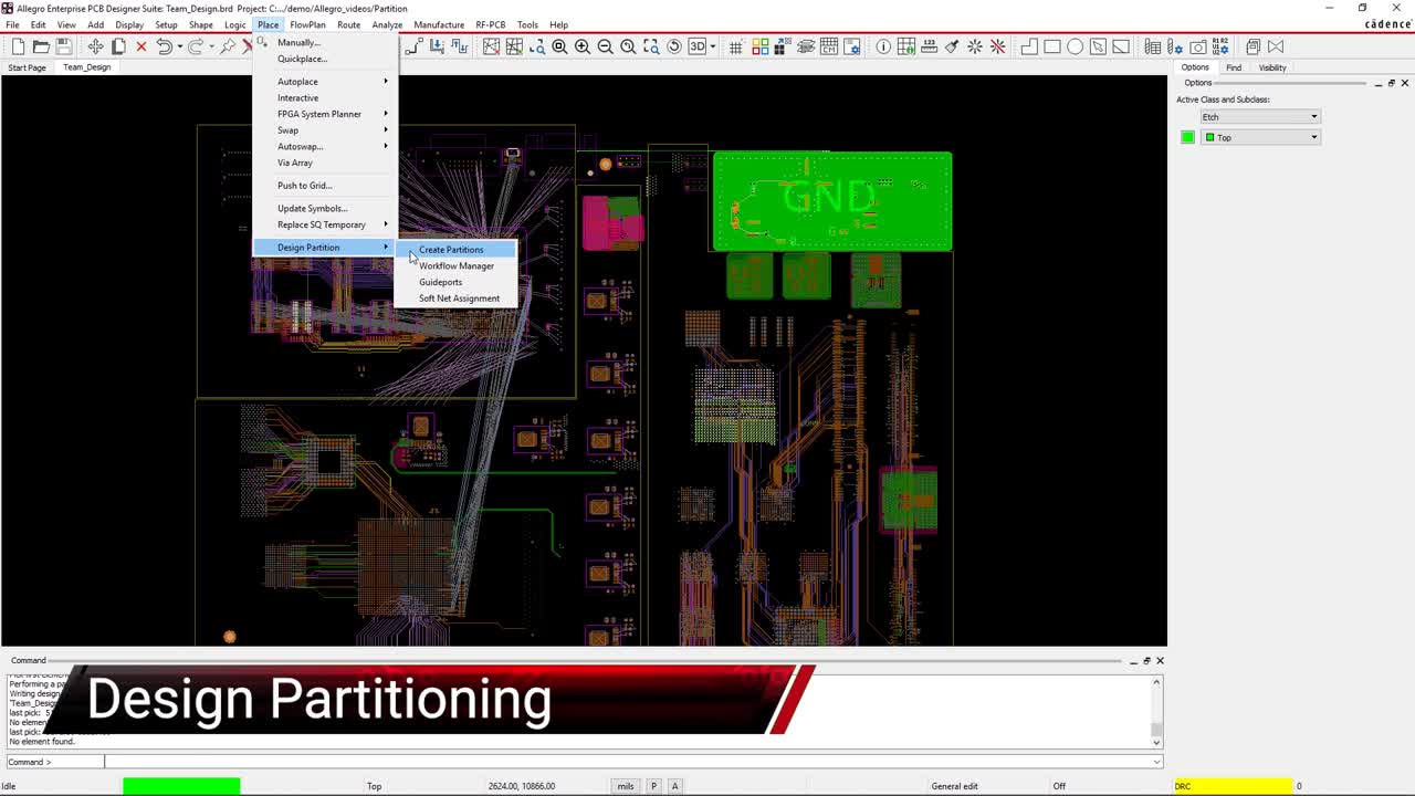
Design partitioning: This option in Allegro allows designers to specify partitions in the layout for team design. Different designers can work on different partitions in the board and then update their work to the master design.
Setting up functional partitioning in your PCB design before you start placing components will give you the organizational foundation that you need for a successful layout. There are many other aspects of PCB design that we can help you with as well, such as the fundamentals of routing traces and creating power and ground planes. You can read more about those in this E-book.
If you’re looking to learn more about how Cadence has the solution for you, talk to us and our team of experts.