Length Matching for High Speed Signals in PCB Design
Key Takeaways
-
Precise timing alignment is crucial for high-speed signals, making length matching especially important in synchronous and differential signal paths.
-
Signal propagation delay and acceptable skew depend on signal frequency and receiver tolerances.
-
OrCAD X enables effective trace length control for differential pairs with constraint management, and delay tuning.
Length matching for high-speed signals, especially high-speed protocols, is essential.
PCB trace length mismatches can lead to serious problems in your design, from signal integrity issues to timing errors that surface long after post-deployment. But when should PCB traces be of equal length, and how much tolerance is acceptable to the difference in length? Read on as we discuss PCB length matching for high-speed signals.
PCB Length Matching for High-Speed Signals
PCB length matching for high-speed signals ensures two or more signal traces are the same length. The question that begs an answer is: what types of traces need matching?
To understand PCB trace matching, you’ll need to forget the ideal concept of electronics, where the receiver immediately receives any waveform initiated by a transmitter. Theoretically, we have assumed that clocked signals have zero time gap and will be processed concurrently at the receiver.
But in reality, the pulses on a bus may not arrive concurrently at the receiving pins if there is a degree of mismatch in the length of the PCB traces. PCB trace length matching ensures that these traces, where the timing of the arrival of the pulses is critical, are matched to equal length; this takes place primarily in high-speed circuits.
Why PCB Trace Length Matching Matters
If your idea of PCB routing neglects PCB trace length matching, you’re putting the entire design at risk. It doesn’t matter if the DRC check tells you all your routing is complete; if buses or differential signals take different paths, you will have some cleanups to do later. While different paths may lead to the same destination, this doesn’t guarantee the same average dielectric constant or electromagnetic interference (EI) for the receiving components. This case is specifically true for synchronous protocols like SPI, I2C CAN, ISA, ATA, and PCI.
Synchronous protocols require precise timing between the clock and data signals. The data must be stable within a timeframe, and transitioning the clock signal will latch the data to the receiver. A clock skewing mismatch happens when the clock and data traces have different lengths. Clock skew may lead to the wrong state of data being latched and affecting the functionality of the electronics.

PCB trace length mismatch can result in clock skew.
Besides synchronous signals, PCB length matching for high-speed signals is also necessary for differential signals. Differential signals work on the assumption that both traces are completely opposite in amplitude. Having similar trace lengths keeps timing differences to a minimum and prevents electromagnetic interference (EMI) from unanticipated ground current flow from the mismatch.
At What Frequency Should You Worry About PCB Trace Length Matching
Depending on the difference between the PCB trace lengths and the speed of the traveling pulse, you can estimate if there will be any issues by focusing on signal integrity. As you’re probably aware, signals travel on PCB traces with a certain speed. This parameter is known as the propagation delay. Communication signals operate at different frequencies, and you can get the clock period by inverting the frequency value.
Measure propagation delay in time per unit of length; you can estimate the total mismatch length to get the resulting skew duration. Then, you’ll refer to the receiver component's datasheet and acquire the tolerance in the timing for the data setup, latch, and hold for a valid cycle.
If the skew duration falls within the tolerance window, you will unlikely encounter any complications. Below is a concise table that has some rules of thumb:
Rule-of-Thumb Guidelines for PCB Signal Propagation Delay and Trace Length Matching
|
Signal Frequency |
Clock Period (T) |
Max Skew Tolerance (20% T) |
Propagation Delay |
Max Trace Length Mismatch |
|
100 MHz |
10 ns |
2 ns |
~150 ps/in (FR4) |
~13 in |
|
200 MHz |
5 ns |
1 ns |
~150 ps/in |
~6.7 in |
|
500 MHz |
2 ns |
0.4 ns |
~150 ps/in |
~2.7 in |
|
1 GHz |
1 ns |
0.2 ns |
~150 ps/in |
~1.3 in |
|
2 GHz |
0.5 ns |
0.1 ns |
~150 ps/in |
~0.67 in |
|
5 GHz |
0.2 ns |
0.04 ns |
~150 ps/in |
~0.27 in |
Note that propagation delay on FR4 PCB material is typically around 150 ps/in (or ~6 in/ns), with a skew tolerance set to ~20% of the clock period—a common conservative rule. Real limits depend on receiver setup/hold timing and signal rise time.
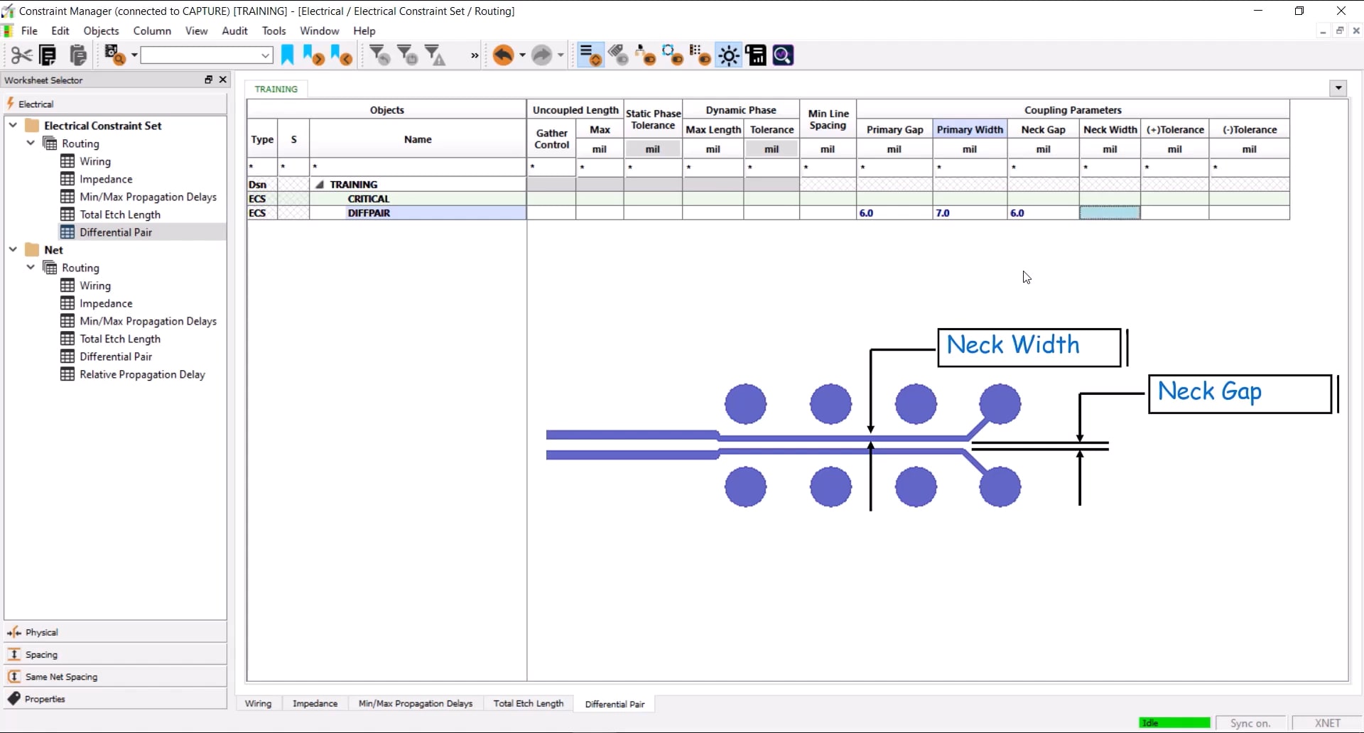
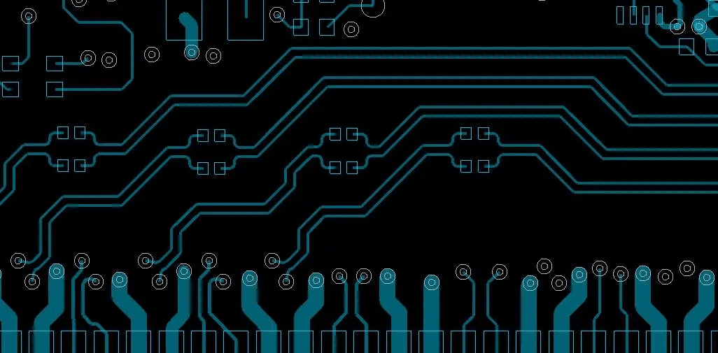
The OrCAD X constraint manager allows for easy length matching of differential pairs.
OrCAD X Features for Length Matching
With the right PCB software, length matching for high-speed signals is easy. The length matching feature in OrCAD X allows you to keep the length of PCB traces within a tolerance value.
|
Feature |
Description |
|
Enables designers to define and enforce length-matching constraints across nets, differential pairs, and buses, ensuring synchronized signal transmission. |
|
|
Allows for the creation of matched groups with specific delay constraints, ensuring signals within the group arrive simultaneously at their destinations. |
|
|
It supports the precise routing of differential pairs with real-time phase control and dynamic phase adjustments to maintain signal integrity. |
|
|
Provides 18 different tuning patterns, such as trombone and sawtooth, to adjust trace lengths accurately, accommodating various layout requirements. |
|
|
Inclusion of Pin and Via Delays |
Accounts for delays introduced by component pins and vias in length matching calculations, providing a more accurate assessment of signal timing. |
Length matching for high-speed signals is essential for preventing skew and preserving timing integrity across your design. Cadence's OrCAD X PCB design platform offers integrated constraint management, delay tuning tools, and real-time differential pair routing to support accurate trace length alignment. Try it yourself with a free OrCAD X trial and maintain signal integrity at every stage of your PCB layout.
Leading electronics providers rely on Cadence products to optimize power, space, and energy needs for a wide variety of market applications. To learn more about our innovative solutions, subscribe to our newsletter or our YouTube channel.