01 - Smart Placement Using Design for Assembly Tools
Design For Assembly is a good place to start since our boards go through placement before there is any actual routing activity. Meanwhile, the real world turns this around starting with the fabricated printed circuit board and adding value from there.
This Design For Assembly feature goes back about 12 years. Let’s go over the routine for setting up the PCB footprints for dynamic spacing. Start with the premise that each component footprint has an assembly outline as well as what’s defined as the Package_Geometry Place_Bound-Top layer. That is usually expanded beyond the edges of the component outline.
The original idea was that the Place_Bound layer was used to define the courtyard which is the minimum amount of personal space around a part. For minimum spacing, you would line up one part’s shape right next to the others. If you wanted to know where any remaining space was left on the board, you turn on the Place_Bound layer. Open space was wherever the shapes were not covering the screen.
I mention that because a lot of the old timer Designers were quite attached to the Place_Bound layers as a means of determining where there was room to move into so that the congested area could be improved in some way. The issue with that approach is that the 3D imagery and the mechanical export of the data didn’t show the actual size of the part as it included the keep-out area around each part. I could put six caps together in a 2x3 grid and you would see a monolithic shape from all six parts that looked like one big part.
I’m triggered by that because it sends ambiguous messages to the mechanical design team. I’d like it if all of the components had a step model so that the 3D images were closer to a render of the actual board. Sometimes, you just can’t find the step model. Like when your company builds its own part, who is going to create a step model?
Here’s what I do for component creation:
- Draw the Place_Bound shape the same size as the nominal assembly outline; no expansion and no accounting for pads.
- Set a property for the minimum and maximum component height or just go with nominal as the max.
- Draw rectangles (or whatever) for each pad that extends beyond the body of the component. I’d start with a single pad so I could give it a low height, 25 to 50 micrometers as you are representing the height of the copper above the outer dielectric layers. Copy that pad wherever it’s needed. You don’t want to go back and edit every shape for the height so do that first and then make the copies.
- Add a DFA property to the “Drawing”. Let me walk you through this part.
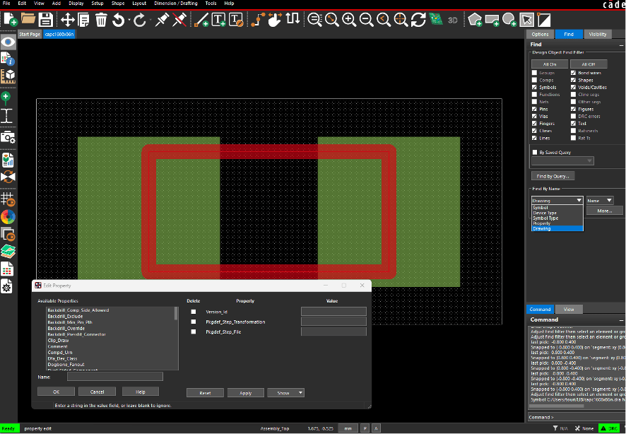 Figure 1. A typical legacy 0402 footprint showing pads (green) part outline (red) and Package_Geometry Place_Bound_Top layers. Three new Place_Bound shapes will represent the component and the two pads for a more precise 3D image and/or MCAD export. The DFA process will be where component spacing rules are enforced.
In order to get to the little window at the bottom, you have to run the Edit > Properties command and then click on the Find by Name option at the bottom of the Find Filter. To begin with, it usually shows the Symbol option but you have to go to the bottom of the pull-down and select Drawing. It’s difficult to find this just by poking around but you get used to it.
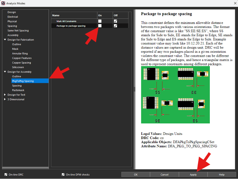 Figure 2. Once the library footprints include both the DFA shape and property, you can enable the DFA rules using Setup > Constraint Modes and then finding and enabling Pkg To Pkg Spacing.
When you’ve selected Drawing, the list comes up and you will find the option for Dfa_Dev_Class in the alphabetically sorted list. Once you’ve clicked on the Dfa_Dev_Class option, you can add an appropriate class to the drawing. I don’t recommend functional names like SOT or BGA.
What has worked for me is figuring out how much the Package_Geometry Place_Bound layer grows beyond the extents of the part and using a numeric value that describes the distance between the Place_Bound layer and the outer edges of the part geometry, including pads as they may protrude. It may not always be symmetric so just use rounded off numbers to Z-copy and reduce the DFA shape from the Place_Bound shape.
The case above in Figure 1 has a Place_Bound expansion of 250 microns for the courtyard. What I would do is first copy the Place_Bound_Top layer to Package_Geometry Display_Top layer. This is for the people who want to live in the past and get that visual proof of where there is room left in the placement. They can use these shapes the same way as was used for the Place_Bound layer which will now take on the nominal size of the component body. I usually create a layer of artwork that is not sent to the vendor but uses the Package_Geometry Display layer rather than the Place_Bound layer as the courtyard.
You won’t see a component-to-component spacing error anymore unless two parts actually overlap. The means of separating the components come from a table where all of the Dfa_Dev_Class options can be imported. This is where the number values shine. Each value used by the symbol footprint library creates a column and a row in the table so the fewer you use, the better. Filling out the numbered table involves adding up the two rank and file numbers and putting that value at the intersection of the row and column.
Setting up the Component Spacing Values
This is where you find out why I like to use numbers as the key to setting up component spacing rules. Another factor is using the Z-Copy command with an offset to uniformly shrink the DFA_Bound shape from the Place_Bound_Top shape. The goal is to make it easier to set the DFA table up so that it works right the first time. The assumption here is that you’re starting with a design that relies on the Place_Bound layers (top and bottom) and moving to the equivalent DFA_Bound layers with minimal disruption.
Let’s break it down into steps:
1. Click on Setup > Constraints which opens the constraint window. The bottom tab of the worksheet selector is for the Manufacturing constraints. It consists of Design for Fabrication, Assembly, and Test and we’re going for the DFA Constraint Set under the Design for Assembly folder. The DFA Constraint Set expands to include Outline, PkgToPkg Spacing and Paste_mask. We’re, of course, going for the second option. When you click on PkgToPkg Spacing, all you get is a notice to Press “+” to “create a new cset.” That’s a mouse thing you will now do if you’re following along.
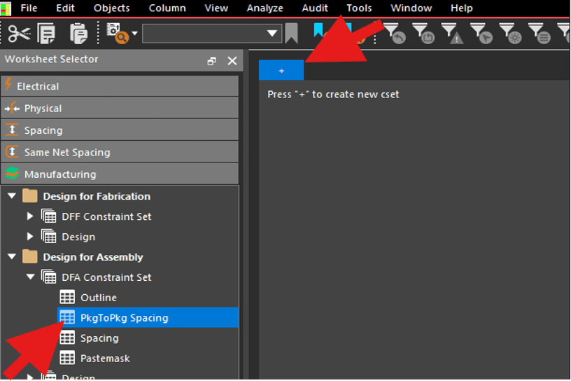
Figure 3. The first time you go to the DFA setup, you start by clicking on the plus sign.
2. Give your CSet a name and click Ok. We flesh it out by going down to the bottom of the page and finding Show symbol classifications.

Figure 4. The DFA classifications of any footprints that have an attribute will be visible and selected in the right-hand column once you’ve picked the Show Symbol Classifications option. After you move your DFA classes to the selected pane, click Ok.
3. The values from the footprint properties will be populated both down and across the resulting table. Filling in each blank requires you to add up the two numbers that correspond to that location. Since the DFA_Bound shape is symmetric with the Place_Bound shape, you can use the same number for all values in the cell. If you type the value once, it will automatically repeat it in the format that allows customization on all sides. I’ve tried to adapt the values to account for an irregular Place_Bound shape. I found it more expedient to just do a uniform reduction of the Place_Bound to make the DFA_Bound shape that uses the same value all around.
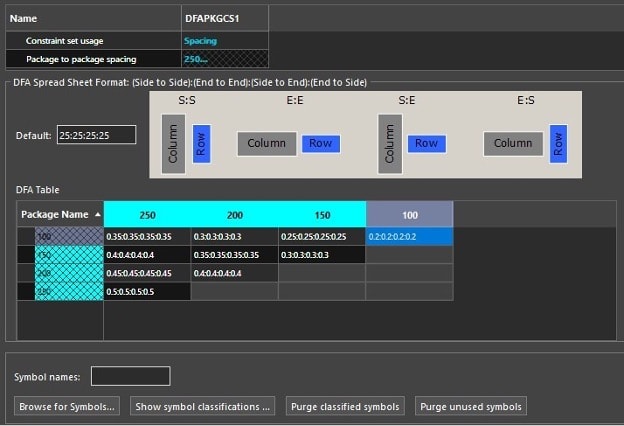
Figure 5. The blue column with the hatch pattern is currently hard to read, however what it’s indicating is that the package spacing rule is applied to the DFA class and not the symbol. In any case, the numbers represent the total of what’s on the outside, kind of like a multiplication table except it’s using the addition function.
The last step is to save the table with a meaningful name related to the density of the board. From here on out, you do not use different footprints to create different spacing rules. Component spacing is controlled by the size of the DFA_Bound shape plus the values in the field. Of course, you will want to test drive the design rules to make sure you have the correct unit of measure and that all of the footprints have the DFA shapes and attributes.
You could also go about this using each footprint rather than classes of footprints but that will lead to a rather large table requiring more clerical work to fill out the spacing rules. One possible way that improves things in the long run goes like this.
When a Test Point Can Be Close to Anything Except Another Test Point
A test point wants a nominal gap from a short component and a little more for a taller component. Beyond that, it wants a larger gap between itself and any other test points. So, you could have a line for the test points where the values are small until it gets to the cell where test point meets test point. Set that one to the value that pleases the bean counters that have to purchase the ICT fixture.
The rest of the values are driven by the assembly people with the potential for wishful thinking from the EE side. Remember, it’s your job to design the board for DFx. When I see DFM, I read “Design For Money”. That may mean that you have to challenge the Assembly team rather than saying “No” to everyone else.
One example of how the DFA process was more suitable was when I started the Chromecast device. Google had a library with the functional categories. The air gaps were set up by the people who design the internet backbone. Those data center boards required more space between parts than we could manage.
Having come from Qualcomm, the minimum spacing I was used to was driven by the cell phone industry. Our component spacing was determined by the minimum soldermask web for the smallest parts. There was some agreement between Qualcomm and Google at that scale but Google’s DFA rules required more room, particularly around the connectors and active devices.
Figure 6. Using revised DFA values for a double sided HDI circuit circa 2014
In this case, I didn’t have to edit the library symbols. What happened is that wherever the spacing value was above 250 microns (10 mils) would be changed to 250 microns. Values that were already lower than that would remain as they were. Just like that, the spacing rules were adapted from rack equipment down to that of a dongle.
Given the chance to create more accurate 3D renders and exports along with the flexibility introduced by using the DFA option is too good to pass up. I had to make this the opening chapter of the story of how using design constraints can lead to high confidence in the board fabrication and assembly processes.
Yes, there is a bit of work on the library to do up front. A good part of the effort is repetitive which means that a script could be written as the first footprint is updated. The next part would start out by playing back the script. Then all you do is check to see if anything needs to be tailored to that footprint before moving on to the next one. This may not seem like a high priority and it is not unless you are the official librarian. Most places will have a lull between product introductions where you need something productive to fill that downtime.
View the next document: 02 - PCB Constraints: Controlling Trace Width Using OrCAD X and Allegro X Tools.
If you have any questions or comments about the OrCAD X platform, click on the link below.
Contact UsClick here to download the PDF.