00 – Introduction to PCB Constraints
I remember my very first PCB designs way back around 1990. We didn’t even use a netlist, let alone a set of embedded design rules. In fact, the tool we used to create the RF amplifiers for the military and the industry was better suited to designing the floorplan of a house than an electronic circuit.
Those printed circuit boards were strictly single layer boards with an unbroken ground plane on the bottom. They were subsequently joined with a so-called pallet that was made of aluminum and bonded to the metalized bottom side of the board. We used the same software to design the circuit and the aluminum underpinning.
Why Constraints Matter
Thus, it was a big deal to finally get to use actual ECAD software to do the multi-layer control boards for the amplifiers. It wasn’t as big of a leap forward as you’d expect, being the early ‘90s and all. In particular, analog circuits will feature some traces that are controlled by their width and also by the air gap to the ground plane. That’s not asking for much.
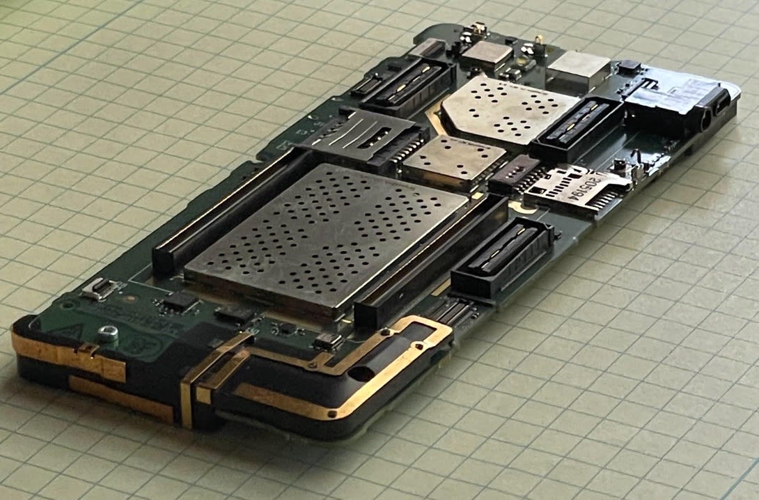 Figure 1. A test mule for various phone features. Size really matters in this space so we need tools that can adapt to the density. Image Credit: Author
Having multiple air gaps was not supported with mid-90s “shrinkwrap” software. What I had to do was temporarily make all of the high frequency traces extra wide and create a ground plane around that geometry. Then, I had to change the RF lines back to their specified width to make Gerber data. Finally we used a Gerber editing tool to remove and replace the original shapes with the ones that were doctored for the novel spacing requirements. Mixing different Gerber layers to get something in between the two is not for those who are risk averse!
Analog vs. Digital Know Your Workarounds
Life in the analog design world became much easier when we could assign properties to nets that allowed a repeatable ground pour that gave extra space where needed and tightened up to the nominal value wherever that applied. Whatever tool we were using, it seemed like the high-speed digital domain got the useful commands and we designers on the analog boards had to be crafty with the shapes to complete our boards.
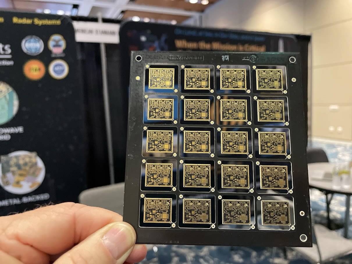
Figure 2. Small form factors give rise to assembly sub-panels that allow several printed circuit boards to be processed in one go. Image Credit: Author
This was way back before the rise of the internet so, obviously, the internet of things didn’t exist. That meant that the majority of designers lived in the digital realm where support for length and width were stronger than support for things like tuning stubs or antennas that connect to the RF lines but also to the ground plane without a break in the metal. So, we had a short to ground at DC frequencies but also an antenna at 2.4 GHz. Doing unusual analog things like that meant that we were compelled to use some kind of undocumented workaround to arrive at the artwork we needed.
The Net Short Property for Joining Two Connections
The good news is that wireless technology has become more mainstream and the PCB Design tools have stepped up with better ways to document the eccentricities of the analog world. For instance, Cadence lets me assign two nets to a shape, via or other element so that it can be used as a short between two nets.
This comes in handy when a small AGND area is tied to the primary GND plane(s) at a single point; probably the most frequent use-case of joining different nets together without having to live with a design rule check (DRC) violation. If at all possible, I’d rather not be in a position where I have to waive a DRC so I look for rules and properties that allow us to tape out a clean design. The net short property is one such avenue.
This is one of many little hooks that can be applied to a Printed Circuit Board design. Every iteration of the software adds more ways to define and control the outcome of our design efforts. The experienced designer knows that the first trace routed will very likely go through several revisions by the time the last trace is drawn.
Even then, when all of the work is done, the board goes to the archive until the day that a new iteration has to be fleshed out. By that time, the database has become something of a stranger. It might even be someone else’s project when the revision hits. That is when capturing the relevant geometries up front helps keep the job from going sideways.
Using the example of a net short is a way to emphasize that the exception to the established rules could be even more important to document than the mundane spacing requirement. Whatever it is that you’re trying to do, there’s probably a way to save the underlying requirements.
Design Constraints - When Is It Too Much of a Good Thing?
Some requirements have multiple ways of being implemented. The length of a trace can be controlled with a minimum and/or maximum length. It could also be part of a group that is length-matched to one of its several members. Two nets can be related as a differential pair and have their own rules governing their behavior with regard to each other. For example, the maximum uncoupled length of the pair can be assigned which would limit the phase-matching bumps. The rules can be at odds with each other, so we have to be careful not to over-constrain the design.
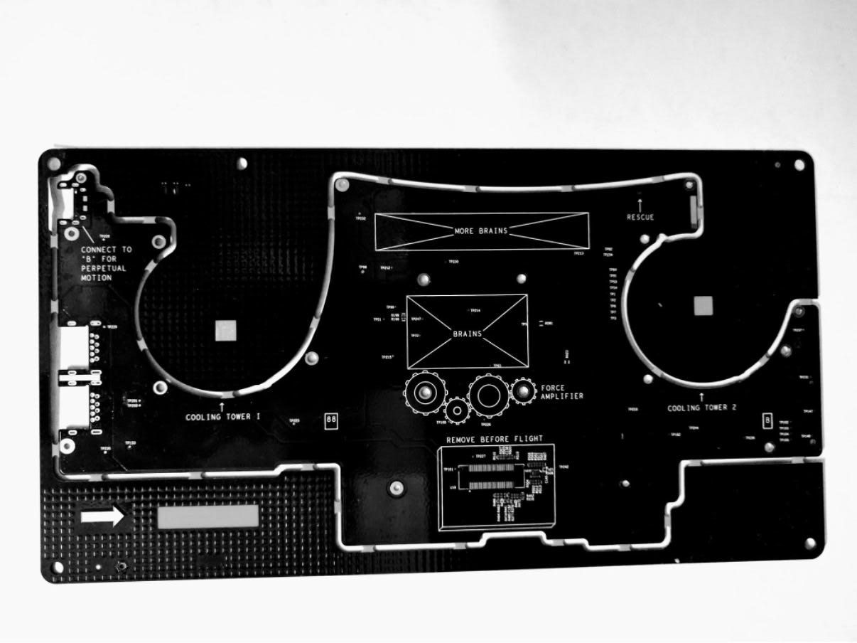 Figure 4. The PCB Outline can have a large impact on the placement and routing challenges. Once in a while, we get to have a little fun with the silkscreen layer. Image Credit: Author
Eventually, the solution may involve compromise where the design rules were aspirational rather than achievable. If you’re given a design where the rules are too restrictive, the team has to hear from you about it. Negotiations on design rules are part of a successful project.
I had a Regulatory Engineer who worked out on the other coast. We were designing edge routers that had the power supply on the same board as the processors. This power circuit had the fist-sized transformer and an inductor almost as large. It’s not often that you see a 12-layer logic board that is also used as a main power supply.
My man from Rochester insisted that there were sufficient rules for the power supply that it would flag anything that did not meet the conditions that he had spelled out on the schematic. That is when I had to up my game on air gaps as well as widths on a pin-to-pin basis. After that, a memory bus seemed easier.
With this introduction, I’m going to jump into placement and routing to shine a light on some of my favorite design constraints using the Cadence OrCAD X/Allegro X Design Platform. The goal is to drive a design that meets the requirements in a way that can be easily verified. The constraint manager is the insurance policy that helps you deliver the goods.
View the next document: 01 - PCB Constraints: Part One - Smart Placement Using Design for Assembly Tools
If you have any questions or comments about the OrCAD X platform, click on the link below.
Contact UsClick here to download the PDF.