USB Design Guidelines with OrCAD X
Key Takeaways
-
Proper impedance matching is critical for USB 2.0 signal integrity, and is achieved through controlled trace geometry, spacing, and material properties.
-
Effective PCB routing for USB involves maintaining matched differential pair lengths, minimizing via usage, and using continuous ground planes to reduce EMI.
-
Design constraints, such as critical length limits, differential pair skew control, and proper termination, are essential for reliable high-speed performance.

Modern electronic systems—from consumer devices to industrial and automotive applications—rely on the Universal Serial Bus (USB) for high-speed data transfer. Designing robust USB interfaces requires careful attention to signal integrity, impedance matching, and precise PCB layout. This article focuses on specific USB design guidelines, including rules and constraints, while using Cadence OrCAD X software.
USB Connector and Pin Design Standards
|
USB |
Pin |
Details |
|
USB 2.0 (Type A and B) |
+5V (Red, VBUS) |
Supplies 5-V power at up to 0.5-A |
|
D– (White) |
Negative USB data line |
|
|
D+ (Green) |
Positive USB data line |
|
|
GND (Black) |
Serves as the ground (0-V) |
|
|
Mini-USB / Micro-USB |
VBUS (Red) |
Supplies 5-V power |
|
D– (White) |
Negative USB data line |
|
|
D+ (Green) |
Positive USB data line |
|
|
ID |
Supports On-The-Go functions, enables role switching between host and peripheral (commonly tied to GND for Type A or left unconnected for Type B) |
|
|
GND (Black) |
Serves as ground (0-V) |
|
|
Shield |
An uninsulated shield cable is typically included to protect against interference (usually not labeled) |
|
|
Universal / USB 3.0 |
USB 2.0 Pins |
Retain their original functions and color coding (VBUS, D–, D+, and GND) |
|
SSTX– / SSTX+ |
Pins for SUPER_SPEED* data transmission |
|
|
SSRX– / SSRX+ |
Pins for SUPER_SPEED* data reception |
|
|
Extra Ground/Shield |
Additional ground/shield configuration to ensure backward compatibility with USB-2.0 devices |
USB Design Guidelines for Impedance Matching
Achieving proper impedance matching is critical for maintaining signal integrity in USB-2.0 high-speed interfaces. The USB standard requires the differential characteristic impedance to be kept at 90-Ω ±15%. This is accomplished by carefully controlling various physical parameters:
Trace Geometry:
-
Trace Width (w): Determines the single-ended characteristic impedance (typically targeted at 45-Ω ±15%).
-
Spacing Between Traces (d): Affects the coupling between the D+ and D– lines. Closer spacing increases coupling and decreases differential impedance. Typically, a 5-mil spacing between differential traces is recommended to optimize coupling and achieve the target differential impedance.
-
Trace Length: While longer traces can increase loss and signal degradation, they must also be matched between the differential pair.
-
Dielectric Height (h) and Constant (εᵣ): The distance from the trace to the ground plane and the PCB material’s dielectric constant also influence the impedance.
Critical Length Considerations
When routing on a 2-layer PCB, one effective strategy to avoid complex impedance matching is to keep trace lengths below a “critical length.” This critical length is based on the allowable input impedance deviation relative to the signal’s rise time.
For a typical FR4 board (with Dk = 4.8), the propagation delay is approximately 150-ps/inch. With a driver rise time of 500-ps (for high-speed USB), the signal travels roughly:
Signal Travel Distance = 500 pc * (1 inch/150 ps) 3 inches
Design rules based on this travel distance are:
-
10% Limit: This is a conservative approach that yields a critical length of 0.3 inches.
-
25% Limit: This more relaxed guideline, commonly used on 2-layer boards, allows for a 0.75-inch critical length.
While these limits help guide routing decisions, they are approximate and can be ambiguous. It is often preferable to design directly to the 90-Ω differential impedance target rather than relying solely on critical length rules.
Differential Pair Skew and Termination
In addition to keeping trace lengths short, maintaining the integrity of differential pairs is crucial:
-
Differential Pair Skew:
USB-2.0 high-speed designs allow a maximum skew of about 100-ps. With an estimated propagation delay of roughly 6-ns/inch (for surface-layer routing), the permissible length mismatch between the D+ and D– traces is approximately:
100 ps *( 1inch/ 6000ps) 0.017 inches/increment
In practice, this results in an allowed mismatch of roughly 0.6 inches (600 mils) across the entire interconnect (board, cable, and receiving board). Although this limit is generous, careful routing is essential to keep the differential pair together and minimize any skew.
-
Proper Termination:
To prevent signal reflections and ensure impedance matching, USB-2.0 specifications require termination resistors on the D+ and D– lines near the connector. Typical resistor values can range from 15-Ω to 45-Ω (for instance, the TUSB2077APTR USB Hub controller uses 27-Ω). It is important to consult the component datasheets to determine the appropriate termination values for your design.
USB-2.0 Specifications
|
Specification |
High Speed (USB-2.0) |
Full Speed (USB-2.0) |
|
Minimum Driver Rise/Fall Time |
500-ps |
4 – 20-ns |
|
Maximum Differential Pair Skew |
100-ps |
1 – 5-ns |
|
Impedance Target |
90-Ω Differential |
90-Ω Differential |
|
Critical Length (10% limit) |
0.3 inches |
2.4 inches |
|
Critical Length (25% limit) |
0.75 inches |
6 inches |
PCB Routing Guidelines for USB- Design
The routing technique depends on your topology and signaling standard, and it must be carefully planned to preserve signal integrity.
For a 2-layer PCB, two techniques are considered:
Coupled Differential Microstrips: Using a layer stack-up calculator, it is found that trace widths of approximately 16 mils with 5 mil spacing between differential pairs can meet the 90-Ω target, even though the single-ended trace width might appear narrower than expected.
Coplanar Differential Microstrips: This involves placing a ground pour alongside the differential traces on the same layer and beneath them on the opposite side. For example, using 9.5 mil wide traces with a 5 mil gap between them and a 5 mil spacing to the adjacent ground plane can also achieve the 90-Ω differential impedance.
Consistent width and spacing must be maintained throughout the route, as USB routing treats the traces as individual single-ended lines carrying a differential signal.
General Routing Considerations
High-speed PCB routing for USB requires meticulous control over trace geometry and layout to ensure optimal signal integrity.
|
Key Routing Guideline |
Details |
|
Trace Length and Topology |
Keep routes as short and direct as possible. Ensure differential pairs are length-matched and routed together using gentle 45° angles or curves instead of abrupt 90° turns, minimizing attenuation and signal reflections. |
|
Design Rules and Signal Integrity |
Establish clear rules such as fixed impedance values, minimal via usage, and proper trace spacing (e.g., differential pairs should be at least five times the trace width apart from other signals). Use continuous ground planes to stabilize impedance and reduce EMI. |
|
Minimal Use of Vias and Length Alignment |
Use vias sparingly to avoid impedance discontinuities; when needed, consider techniques like back-drilling. Ensure equal trace lengths for differential pairs to prevent timing mismatches and reduce signal degradation. |
|
Routing Tools |
Leverage advanced PCB design tools like OrCAD X that integrate impedance calculators and electromagnetic field solvers to automatically analyze trace geometry, suggest optimal widths and spacings, and enforce net-specific design rules. |
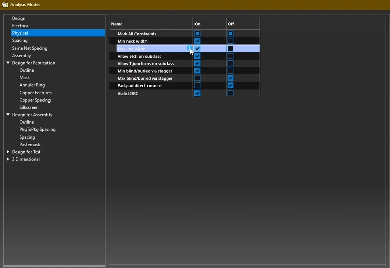
Constraint-Driven USB Design in OrCAD X
OrCAD X supports a robust constraint-driven design and ensures each aspect of USB PCB design meets strict electrical, physical, and high-speed requirements, minimizing design errors and improving performance.
-
Embedded Rule Enforcement:
By incorporating predefined electrical, physical, spacing, manufacturing, and high-speed constraints directly into the design process, OrCAD X automatically enforces rules for trace width, spacing, and differential pair matching, reducing the risk of signal integrity issues. -
Real-Time Design Rule Checks (DRC):
OrCAD X provides real-time feedback on any design rule violations. This immediate validation allows designers to correct issues as they occur, preventing errors from propagating through the design cycle. -
Reusable Constraint Templates:
Designers can create reusable constraint templates using Net Classes, Net Groups, and Regions. These templates ensure that design rules are consistently applied across multiple projects, enhancing repeatability and reducing manual setup time.
Using OrCAD X, you will be able to easily adhere to USB design guidelines, as they combine precise routing techniques with a constraint-driven approach that is seamlessly integrated. Explore how Cadence's PCB Design and Analysis Software and OrCAD X platform streamline constraint setup and ensure reliable PCB performance.
Leading electronics providers rely on Cadence products to optimize power, space, and energy needs for a wide variety of market applications. To learn more about our innovative solutions, talk to our team of experts or subscribe to our YouTube channel.