How to Make a PCB Schematic
Key Takeaways
-
Begin with a clear understanding of inputs, outputs, power needs, and communication protocols to guide component selection and layout.
-
Arrange components in functional blocks with clear signal flow to ensure readability and effective design management.
-
For complex schematics, utilize tools like hierarchical schematics, extensive component libraries, and simulation tools for streamlined creation.
OrCAD X Capture allows users to easily get started with making a PCB schematic.
Designing a PCB schematic is the first major step in PCB design. Learning how to make a PCB schematic begins with an understanding of the requirements. Read on as we discuss the first section of how to create a schematic using OrCAD X.
Basics of How to Design a PCB Schematic
Start by defining the inputs and outputs, identifying key integrated circuits you’ll be using, and detailing the power, voltage, and current needs of your system. Consider any communication protocols your design will use, such as I²C or SPI, and any physical constraints that could influence your component choices or layout. With these parameters in mind, create a block diagram to visualize the high-level flow of power and data through your circuit. This step not only helps clarify the overall design but also guides decisions about required power supply and data flow components.
In every section of the schematic design process, OrCAD X is there to help you:
-
OrCAD X Libraries: Provides extensive libraries of pre-designed components, such as voltage regulators, microcontrollers, and communication ICs, for quick selection.
-
Custom Components: Supports the creation of custom symbols and footprints to accommodate specific requirements.
-
Parameter Management: Includes tools for managing component parameters like voltage, current, and tolerance directly in the schematic editor.
Logical Organization of the Schematic
Once the framework is established, organize your schematic with a logical structure. Schematics typically flow from left to right and top to bottom, with power connections at the top and ground at the bottom. Group related components, such as power regulation circuits, microcontrollers, or sensors, into functional blocks for clarity. For complex designs, hierarchical schematics can simplify the visualization and management of your circuit. OrCAD X offers several features that assist in logically organizing and managing your schematic:
-
Hierarchical Design: Allows the use of block symbols and sub-sheets for organizing complex circuits into manageable sections.
-
Schematic Navigation: Enables seamless movement between levels of the hierarchy to inspect or edit individual blocks.
-
Port and Bus Support: Simplifies signal routing between blocks using named ports and buses.
Connecting the components with wires and nets is the next step, but it’s essential to define design rules and constraints (DRCs) early in the process. This foresight minimizes backtracking and ensures your schematic is ready for simulation and validation. OrCAD X enables you to do all this and more:
-
Constraint Manager: Lets you define design rules, such as spacing and connectivity, directly in the schematic environment.
-
DRC Checks: Automatically detects and highlights design rule violations, such as unconnected pins or short circuits.
-
Net Management: Provides tools to define and manage nets with specific attributes like voltage levels or signal types.
Simulating and Finalizing the Schematic
Simulating your design allows you to verify functionality and catch errors before moving to layout. Once validated, complete the schematic by adding annotations, such as reference designators and labels, to prepare it for the PCB layout stage. Thoughtful planning at every stage of schematic design lays the groundwork for a successful PCB. OrCAD X's simulation and annotation tools streamline these final steps:
-
PSpice Integration: Provides robust simulation capabilities, enabling detailed circuit analysis and validation before physical implementation.
-
Annotation Features: Automates the assignment of reference designators and the addition of descriptive labels to prepare the design for layout and manufacturing.
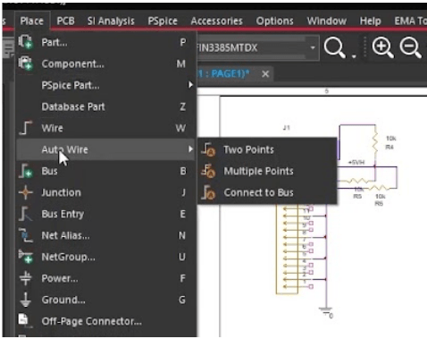
You can automatically wire between components in OrCAD X with Place > Auto Wire > two points
How to Make a PCB Schematic with OrCAD X Capture
Creating a PCB schematic in OrCAD X can be done efficiently using its time-saving features. Follow these steps to ensure accurate connections and a well-organized design, including basic components, ICs, and even buses.
|
Step |
Action |
Description |
|
1. Enable Grid Snapping |
- Click the Snap to Grid button. |
Ensures all component pins align and connections are made accurately. |
|
2. Place Components |
- Use the Place Component feature. |
Drag and drop components into the schematic, aligning them properly on the grid. |
|
3. Wire Components Manually |
- Select Place > Wire. |
Provides manual control for precise wiring. Finish the wire by double-clicking or pressing Escape. |
|
3b. Connect Components Automatically |
- Select Place > Autowire Two Points. - Click the first pin and the second pin to connect them. |
Creates automatic wires between pins. Right-click and select End Mode to finish. Adjust wires to avoid overlapping pins. |
|
4. Use Buses for Parallel Connections |
- Select Place > Bus. |
Simplifies connections in designs with multiple parallel signals. Right-click and select End Wire to finish. |
|
5. Connect Components to a Bus Automatically |
- Select Place > Autowire Connect to Bus. |
Automatically connects pins to the bus.Enter net names to assign sequential numbering for connections. |
|
5a. Add Bus Entries Manually |
- Select Place > Wire. |
Draw manual connections between pins and the bus. Use Place > Bus Entry or press E to add entries, rotating them with R if necessary. |
|
6. Use Net Aliases |
- Select Place > Net Alias. |
Connect wires or pins that cannot be physically connected. The alias name increments automatically for subsequent connections. |
|
7. Save and Validate |
- Save the schematic. |
Regularly save your work and run checks to ensure there are no errors or violations in the schematic design. |
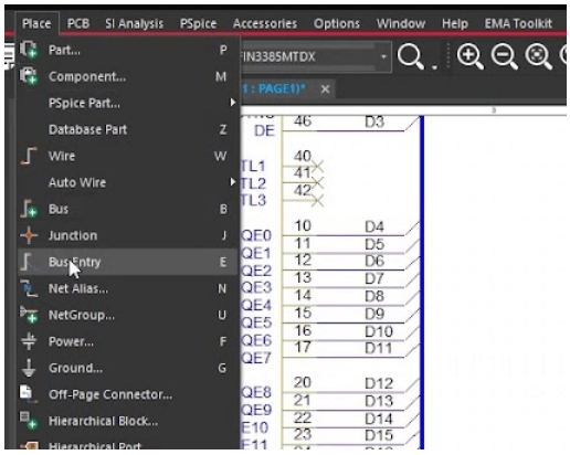
Placing a bus entry in OrCAD X
New Designs With OrCAD X – What to Look Out for
For new designers creating schematics, it is important to know about some of the useful features OrCAD X has for schematic creation.
-
Component Libraries: OrCAD X provides extensive component libraries, offering a selection of pre-designed parts. These libraries facilitate quick component selection and placement, streamlining the design process. Additionally, OrCAD X supports the creation of custom components, allowing designers to tailor parts to specific project requirements.
-
Simulation with PSpice: PSpice comes integrated with OrCAD X and enables designers to simulate and analyze circuit behavior before physical implementation. This simulation capability helps identify potential issues, optimize performance, and validate design functionality.
-
Buses: In complex designs with multiple parallel connections, buses are used to group related signals, simplifying the schematic and enhancing readability. OrCAD X allows for easy creation and management of buses, supporting automatic naming conventions.
-
Design Rule Checks (DRC): OrCAD X includes DRC features that automatically verify the schematic against predefined electrical and physical rules. This ensures compliance with design standards, identifies errors such as unconnected pins or short circuits, and helps maintain the integrity of the design throughout the development process.
-
Hierarchical Design: OrCAD X enables hierarchical schematic design, allowing designers to organize complex circuits into smaller sections. Each section is represented as a block symbol at the top level, providing a bird's-eye view of the design. Designers can navigate between different levels of the hierarchy. OrCAD X resolves net name conflicts and manages unique reference designators, maintaining consistency across all design levels and streamlining the development process.
With OrCAD X, how to make a PCB schematic becomes easy—from defining requirements to simulation and validation. Ready to elevate your PCB designs? Explore Cadence PCB Design and Analysis Software and discover how OrCAD X can streamline your workflow today!
Leading electronics providers rely on Cadence products to optimize power, space, and energy needs for a wide variety of market applications. To learn more about our innovative solutions, talk to our team of experts or subscribe to our YouTube channel.