How to Create a PCB Footprint in OrCAD X
Key Takeaways
-
Symbol Creation: Start by referencing the component datasheet to accurately assign pinouts in OrCAD Capture.
-
Footprint and 3D Model Download: Download the correct 2D footprint and 3D model from sites like SnapEDA for integration into your project.
-
Assigning and Editing Footprints: Use the Edit Properties option to assign or edit footprints, ensuring proper alignment with the symbol.
How to create a PCB footprint in OrCAD X is a fairly straightforward process. You can also select the 3D model in the properties panel of the footprint.
When designing a PCB that requires particular parts, you may need to learn how to create a PCB footprint in OrCAD X. The process involves creating a symbol based on the component's datasheet, assigning the correct pinouts, and then linking the footprint and 3D model to the symbol. In OrCAD X, this workflow is streamlined, providing designers with advanced tools for managing footprints, symbols, and component properties. Read on to learn how!
How to Create a PCB Footprint in OrCAD X
|
Step |
Description |
|
Create the Symbol |
|
|
Padstack Creation |
|
|
Download Footprint & 3D STEP Model |
|
|
Assign the Footprint |
|
|
Switch to PCB Design |
|
|
Add the 3D Model |
|
|
Visualize in 3D |
|
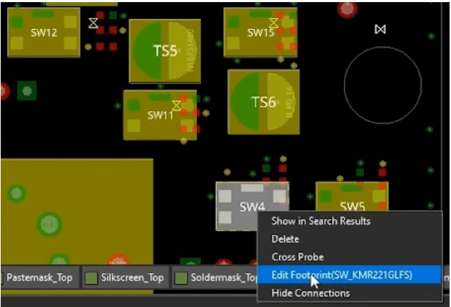
Editing a footprint can be done with right click > Edit Footprint.
Editing a Footprint in OrCAD X
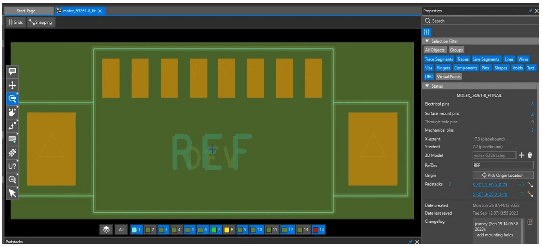
Once you know how to create a PCB footprint in OrCAD X, you may need to further edit a footprint down the line as well. To edit a footprint in OrCAD X Presto, begin by selecting the component and right-clicking to choose "Edit Footprint." If the footprint is stored in your library, it will open in the Footprint Editor. If it’s not in your library, you’ll be prompted to export the footprint from the database to your working directory for editing.
Once exported, a new Footprint Editor window opens alongside your original layout database, where edits are applied. After making adjustments, such as moving pins, updating place bounds, or replacing pad stacks, save the changes and close the editor. The layout editor will then recognize the updates and prompt you to apply them. Options will include updating text, removing fanout, or refreshing pad stacks. Once confirmed, the updated footprint is applied across the entire layout, reflecting the changes in every instance of that component.
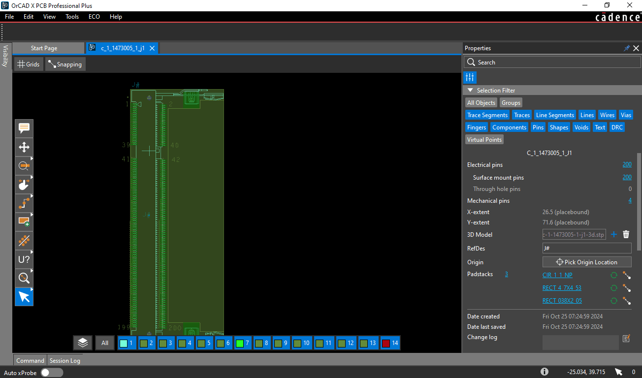
OrCAD X Footprint Editor with properties panel on the right.
OrCAD X Footprint Authoring
The OrCAD X footprint editor is designed for efficient and detailed footprint creation. The Properties panel offers a comprehensive overview of a footprint, including the number and type of electrical and mechanical pins, the reference designator, 3D model access, and a list of pad stacks, which can be updated or replaced as needed
Additionally, the panel includes a change history log for tracking modifications. When adding pins, you can search your pad stack library, view detailed pad stack parameters, and select the appropriate one for your design. If a new pin is required, you can create a pin pad stack parametrically by specifying dimensions for surface-mount or through-hole pin types. Pins can be placed using adjustable grids or by snapping to specific points in the design, with the Properties panel automatically updating to reflect the new additions.
Adding Multiple Footprints In OrCAD X
To add multiple footprints to a component in OrCAD X Capture, start by placing a component that supports multiple footprints.
-
In the Component Explorer, search for your part via description or part number.
-
If prompted, enter your credentials.
-
Once selected, view the available footprints in the properties tab, where you can see all associated symbols and footprints.
-
Place the component in the schematic, adjusting the reference designators if necessary to avoid conflicts. For example, if you have multiple instances of the same component, make sure to update the reference designators to unique values.
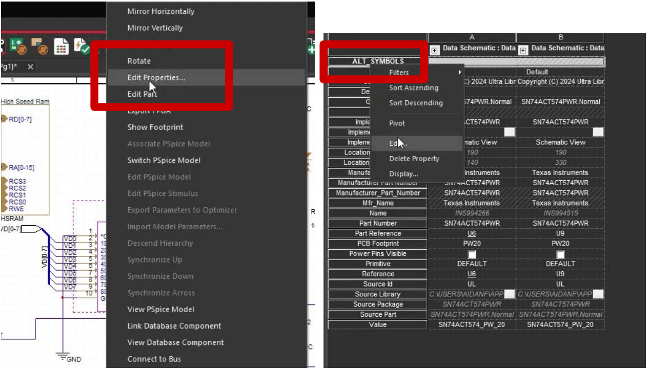
Adding alternate symbols in OrCAD X, make sure to create the ALT_SYMBOLS property before editing it.
In OrCAD X Capture, right-click the component and select "Edit Properties" to assign alternate footprints. In the Property Editor, add a new property labeled ALTSYMBOLS, entering the alternate footprint values. Once applied, use Ctrl to select multiple components and repeat the process for additional instances.
To sync the alternate footprints with the PCB layout, save your design and select "Update Layout." This opens OrCAD X Presto, where you can apply the changes. After syncing, place the components on the board using the placement tool, selecting each footprint from the dropdown in the properties panel. This ensures that the alternate footprints are correctly applied for different board form factors or variations.
As a whole, knowing how to create a PCB footprint in OrCAD X is important when using particular components. OrCAD X features an advanced footprint editor and integrated design environment to streamline the process, making it easier to manage even the most complex designs. Explore more about Cadence's PCB Design and Analysis Software and see how OrCAD X can enhance your PCB design workflow.
Leading electronics providers rely on Cadence products to optimize power, space, and energy needs for a wide variety of market applications. To learn more about our innovative solutions, talk to our team of experts or subscribe to our YouTube channel.