My Four Biggest Mistakes as a PCB Designer
There’s an old saying among test pilots. “Any landing that you can walk away from is a good landing.” They also know that there are old pilots, there are bold pilots but no old, bold pilots - or so the saying goes. If you want to hang around as a PCB designer, you can only hope to walk away from your mistakes with your career intact. So, this is a chance to learn from my mistakes from 35 years of design work.
Going all the way back to the ‘90s finds me in my first PCB Design role. I had just done an internal transfer into the commercial side of the business after a couple of years of feeding from the Government trough. My manager, Merrill, on the Mil-Spec side was a father of a dozen children and was an all-around nice guy; perhaps a bit of a push-over.
Before applying for the transfer, I wanted to have a talk with Merril so I came up behind and asked if he wanted to go to Armadillo Williy’s, a local barbecue place, for lunch. I didn’t see that he had a sandwich in his hand and was about to take the first bite. Instead, the sandwich hit the desk with a thunk and we were off to the restaurant. Such was his dedication to his people.
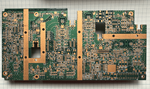
Figure 1. A multi-layer control board for RF amplifiers circa 1999. By that time, I had done many of these and was able to turn them around pretty quickly. Image Credit: Author
A little background: We recently had an audit from the Army and there were many concerns brought up. I was fresh out of a six month program at the Copper Connection. This was a local PCB/CAD trade school that taught the Department of Defence drawing standards along with AutoCAD. I knew my stuff well enough that one of our Mechanical Engineers asked me if I had a photographic memory. No, I had just put in the six months to study the Drawing Requirements Manual.
And so it was that my drawings were cleanest among the several CAD designers with only two flags on my drawing package. One was about hardware call-outs. I was labeling threaded holes with a commercial designation. So I called out a 4-40 UNC-2B threaded hole when it should have been .112-40 UNC-2B. That leading “4” was the same issue we all had where the auditors wanted a diameter value instead. That was an easy one.
1. Assembly Drawings do Not Tell You How, Only What
The other issue was with what the auditors called “methodized drawings”. At the time, Merrill asked me what that meant. My reply was to mention the design reviews where the Manufacturing Engineer would request a list of notes to add to the assembly drawings. The good intention was to have a single document that could be used by the assemblers to stuff the boards. I reminded Merril of all of the times I had pushed back on those requests but was overruled. Lesson learned.
The noble idea was to keep the assembly workspaces tidy. It also made the drawings (what is) into a procedure (how to). The government has reasons to avoid entangling the two.
The outcome of that audit was that, from that day onward, I was tasked with checking everyone’s drawings for compliance with the manual. I had already spent time doing quality control inspection of PCBAs on the assembly line and eventually bare PCBs in the Receiving Inspection Lab. This Checker distraction is going to cut into my productivity!
Before looking at the first drawing, I already knew this was going to be a thankless job. As the newest, most junior person there, I wasn’t going to endear myself to anyone by nitpicking their work. So, in the end, that come-up to putting my name in the Checked By box was a wedge that had me looking over the cubicle wall towards the other team who were enabling 3G wireless technology for the masses.
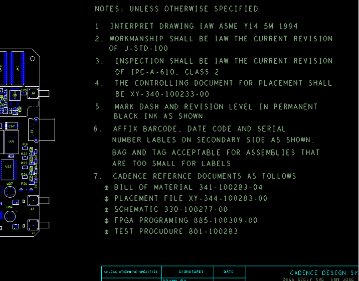
Figure 2. Here is my idea of what makes up an appropriate list of notes. Any instructions on the assembly drawing should be verifiable after the fact by checking the condition of the PCBA. How would we know, for instance, if the assembler used their ESD strap and ionizer while doing their job. Image Credit: Author
Looking back on all of that, I should have brought my Drawing Requirements Manual to the design review with the part about drawings vs. procedures bookmarked for reference. Having solid facts from a reliable source is better than “just my opinion”. Now, we have the internet where getting that kind of information is trivial.
Merill was unable to talk me out of applying for the transfer though he tried. My new manager, Ed, approved and I moved to the other side of the building. As an aside the new job was doing multi-layer boards where everything on the DOD side was single sided power amplifier boards. The Control boards were always outsourced from either side. That was about to change and I was going to be the one to make it so.
2. Crowding Components is Bad No Matter Whose Idea it is
My buddy Joe warned me that “Ed don’t take no shit.” and I was like, “Why should he?” Then he relayed that when Ed was asked what would happen if I could not design multi-layer boards, his reply was, “Then I’ll fire him.” Now, right there is a useful data point. After three days training on some actual PCB design software, I was cut loose on my first 4-layer job. I taped out four layers, no mask, no silk, no clue! That all came together on my second control board.
The commercial group was growing and hired a big brain kind of guy named Dave for that second board. Note that Dave was eventually promoted to VP of Engineering over everyone else. He had a persuasive nature and convinced me that two resistors had to be super-close together or the PLL circuit would not work. I wanted it to work so I nudged them closer and closer until Dave said, “That’s good.”
Dave was wrong and by listening to him, I was also wrong. I’ve told this part of the story before so it may seem familiar with anyone who has known me for the past several years. Ed calls me into his carpeted office and tells me to shut the door and then to sit down. It went something like this.
Ed: Manufacturing is reporting solder issues with a couple of parts on your board. Do you know that we need a solder dam between every pin?
Me: Um, yes.
Ed: So, why do these two parts have their pads too close for that?
Me: Oh, Dave told me that is what is necessary for the PLL …
Ed: (cutting me off) If I want Dave to design the board, then I don’t need you. These boards have to be manufacturable or there’s no point.
Me: gulp. Ok.
Ed: Alright, go back to work but don’t ever do this again.
At least, I got to keep my job for another eight years. So, that never happened again. Not at that first job, nor any subsequent job over the following three decades. Working for startups is all I did until Qualcomm bought one of them. That is where big company processes (and politics) come into play.
3. Learning Big Company Politics the Hard Way
I was having a hard time getting any guidance on shield footprint standards. I had hit up the San Diego based Manager of the mechanical engineering team hoping to learn more. Enough time had passed that I sent a second message letting her know that I was feeling left out about the lack of feedback.
That message totally backfired. It was something I picked up in a course called Managerial Interpersonal Effectiveness (MGMT101). We were instructed not to use a “You” message but rather an “I” message letting the other party know how their behavior is affecting you. That Mechanical Engineering Manager “schooled” me on etiquette and BCC’ed my Manager besides. Yep, another call to the carpet when a simple phone call may have done the trick. I did not see that one coming.
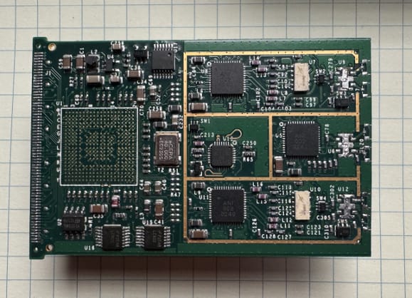
Figure 3. A PCIe based MIMO radio PCB featuring a multi chamber EMI shield. Image Credit: Author
Following that incident, a lot of good things came out of working six years for Qualcomm. One was that they had a really good offshore PCB vendor. I’ll name names. It was Plotech. They had the chops to deliver on smartphone grade PCBs. They were, at that time, a top 100 global PCB vendor but down the list far enough that they were not monopolized by one of the mega-players in the industry. They would treat us well even though Qualcomm was only doing pilot programs to generate reference designs.
4. Using a Taiwan Based Vendor Without Understanding the Customs Process
My next opportunity was at Google’s Chrome OS hardware team. Not long after getting there, the procurement lady moved to a different division. We were told to do our own purchasing until the role was filled. I had a radio board that would be perfect for Plotech so I contacted them to save some money over what the local shops would charge. Even though my email ended with @google, they asked if my company had a website to see if we were legit. Yeah, you might have heard of us!
So, we set up a Non-Disclosure Agreement and I got the quote and ordered a batch of bare boards. I circled back to them a few days after the boards were supposed to ship to get a status on the order. That’s when I learned about customs. You have to lay the groundwork before you can import electronics to this country. In hindsight, a local vendor would have been just fine; not like the company didn’t have the money to spend. That cost the development team about a week where a one-day slip is still a failure.
A bonus mistake that I could walk away from was the time I did a favor for a coworker by cleaning up the reference designators for the silkscreen and the assembly drawing. I pulled the design from the repo and wrote a script while I organized the text and then pushed my script to the repo so he could straighten it all out by repeating my work on his database.
Well, the find filter had changed in between me pulling and pushing and instead of moving the text, it moved almost every part on the board. He had the “stretch” command going so it also contorted the traces while it was at it. Of course, he saved first but we let it run its course so we didn’t hang up the license server or whatever. It was a good time to go get some of that free food even though watching it destroy the layout was indeed hilarious!
This could easily have been five or ten problems I’ve caused. The general idea is that communication is really important. If you’re uncomfortable with something, share your discomfort but don’t surface a problem without offering a solution or two. Circle back with the team early and often to make sure you stay on track. Educate yourself on what the vendors can and can’t do. Use nice words in case you have to eat them later. This all should be part of your nature if you like doing PCB Design.