16 - Digital Worst-Case Timing Analysis
Digital worst-case timing
Manufacturers of electronic components generally specify component parameters (such as propagation delays in the case of logic devices) as having tolerances. These are expressed as either an operating range, or as a spread around a typical operating point. The designer then has some indication of how much deviation from typical one might expect for any of these particular component delay values.
Realizing that any two (or more) instances of a particular type of component may have propagation delay values anywhere within the published range, designers are faced with the problem of ensuring that their products are fully functional when they are built with combinations of components having delay specifications that fall (perhaps randomly) anywhere within this range.
Historically, this has been done by making simulation runs using minimum (MIN), typical (TYP), and maximum (MAX) delays, and verifying that the product design is functional at these extremes. But, while this is useful to some extent, it does not uncover circuit design problems that occur only with certain combinations of slow and fast parts. True digital worst-case simulation, as provided by PSpice A/D, does just that.
Other tools called timing verifiers are sometimes used in the design process to identify problems that are indigenous to circuit definition. They yield analyses that are inherently pattern-independent and often pessimistic in that they tend to find more problems than will truly exist. In fact, they do not consider the actual usage of the circuit under an applied stimulus.
PSpice A/D does not provide this type of static timing verification. Digital worst-case timing simulation, as provided by PSpice A/D, is a pattern-dependent mechanism that allows a designer to locate timing problems subject to the constraints of a specific applied stimulus.
Digital worst-case analysis compared to analog worst-case analysis
Digital worst-case timing simulation is different from analog worst-case analysis in several ways. Analog worst-case analysis is implemented as a sensitivity analysis for each parameter which has a tolerance, followed by a projected worst-case simulation with each parameter set to its minimum or maximum value. This type of analysis is general since any type of variation caused by any type of parameter tolerance can be studied. But it is time consuming since a separate simulation is required for each parameter. This does not always produce true worst-case results, since the algorithm assumes that the sensitivity is monotonic over the tolerance range.
The techniques used for digital worst-case timing simulation are not compatible with analog worst-case analysis. It is therefore not possible to do combined analog/ digital worst-case analysis and simulation and get the correct results. PSpice A/D allows digital worst-case simulation of mixed-signal and all-digital circuits; any analog sections are simulated with nominal values.
Systems containing embedded analog-within-digital sections do not give accurate worst-case results; they may be optimistic or pessimistic. This is because analog simulation can not model a signal that will change voltage at an unknown point within some time interval.
Starting digital worst-case timing analysis
To set up a digital worst-case timing analysis:
- In the Simulation Settings dialog box, click the Options tab.
- Select the General node in the Gate-level Simulation tree Structure of the Options tab.
- In the Timing Mode frame, check Worst-case (min/max)
- In the Initialize all flip-flops drop-down list, select X.
- Set the Default I/O level for A/D interfaces to 1.
- Click OK.
- Start the simulation.
Simulator representation of timing ambiguity
PSpice A/D uses the five-valued state representation {0,1,R,F,X}, where R and F represent rising and falling transitions, respectively. Any R or F transitions can be thought of as ambiguity regions. Although the starting and final states are known (example: R is a 0 → 1 transition), the exact time of the transition is not known, except to say that it occurs somewhere within the ambiguity region. The ambiguity region is the time interval between the earliest and the latest time that a transition could occur.
Timing ambiguities propagate through digital devices via whatever paths are sensitized to the specific transitions involved. This is normal logic behavior. The delay values (MIN, TYP, or MAX) skew the propagation of such signals by whatever amount of propagation delay is associated with each primitive instance.
When worst-case (MIN/MAX) timing operation is selected, both the MIN and the MAX delay values are used to compute the duration of the timing ambiguity result that represents a primitive’s output change.
For example, consider the model of a BUF device in the following figure.
U5 BUF $G_DPWR $G_DGND IN1 OUT1 ; BUFFER model
+ T_BUF IO_STD

.MODEL T_BUF UGATE ( ; BUF timing model
+ TPLHMN=15ns TPLHTY=25ns TPLHMX=40ns
+ TPHLMN=12ns TPHLTY=20ns TPHLMX=35ns)
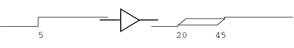
Figure 16-1 Timing ambiguity example one.
The application of the instantaneous 0-1 transition at 5nsec in this example produces a corresponding output result. Given the delay specifications in the timing model, the output edge occurs at a MIN of 15nsec later and a MAX of 40nsec later. The region of ambiguity for the output response is from 20 to 45nsec (from TPLHMN and TPLHMX values). Similar calculations apply to a 1-0 transition at the input, using TPHLMN and TPHLMX values.
Propagation of timing ambiguity
As signals propagate through the circuit, ambiguity is contributed by each primitive having a nonzero MIN/MAX delay spread. Consider the following example that uses the delay values of the previous BUF model.
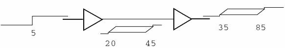
Figure 16-2 Timing ambiguity example two.
This accumulation of ambiguity may have adverse effects on proper circuit operation. In the following example, consider ambiguity on the data input to a flip-flop.
![]()
Figure 16-3 Timing ambiguity example three.
The simulator must predict an X output, because it is not known with any certainty when the data input actually made the 0-1 transition. If the cumulative ambiguity present in the data signal had been less, the 1 state would be latched up correctly.
Figure 16-4 illustrates the case of unambiguous data change (settled before the clock could transition) being latched up by a clock signal with some ambiguity. The Q output will change, but the time of its transition is a function of both the clock’s ambiguity and that contributed by the flip-flop MIN/MAX delays.
![]()
Figure 16-4 Timing ambiguity example four.
Identification of timing hazards
Timing hazard is the term applied to situations where the response of a device cannot be properly predicted because of uncertainty in the arrival times of signals applied to its inputs.
For example, Figure 16-5 below shows the following signal transitions (0-1, 1-0) being applied to the AND gate.
![]()
Figure 16-5 Timing hazard example.
The state of the output does not (and should not) change, since at no time do both input states qualify the gate, and the arrival times of the transitions are known.
Convergence hazard
In cases where there are ambiguities associated with the signal transitions 0-R-1 and 1-F-0—which have a certain amount of overlap—it is no longer certain which of the transitions happens first.
The output could pulse (0-1-0) at some point because the input states may qualify the gate. On the other hand, the output could remain stable at the 0 state. This is called a convergence hazard because the reason for the glitch occurrence is the convergence of the conflicting ambiguities at two primitive inputs.
Gate primitives (including LOGICEXP primitives) that are presented with simultaneous opposing R and F levels may produce a pulse of the form 0-R-0 or 1-F-1.
For example, a two-input AND gate with the inputs shown in Figure 16-6 below, produces the output shown.
![]()
Figure 16-6 Convergence hazard example.
This output (0-R-0) should be interpreted as a possible single pulse, no longer than the duration of the R level.
The actual device’s output may or may not change, depending on the transition times of the inputs.
Critical hazard
It is important to note that the glitch predicted could propagate through the circuit and may cause incorrect operation. If the glitch from a timing hazard becomes latched up in an internal state (such as flip-flop or ram), or if it causes an incorrect state to be latched up, it is called a critical hazard because it definitely causes incorrect operation.
Otherwise, the hazard may pose no problem. Figure 16-7 below shows the same case as above, driving the data input to a latch.
![]()
Figure 16-7 Critical hazard example.
As long as the glitch always occurs well before the leading edge of the clock input, it will not cause a problem.
Cumulative ambiguity hazard
In worst-case mode, simple signal propagation through the network will result in a buildup of ambiguity along the paths between synchronization points. See Glitch suppression due to inertial delay. The cumulative ambiguity is illustrated in Figure 16-8.
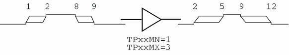
Figure 16-8 Cumulative ambiguity hazard example one.
The rising and falling transitions applied to the input of the buffer have a 1nsec ambiguity. The delay specifications of the buffer indicate that an additional 2nsec of ambiguity is added to each edge as they propagate through the device. Notice that the duration of the stable state 1 has diminished due to the accumulation of ambiguity.
Figure 16-9 shows the effects of additional cumulative ambiguity.
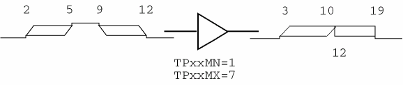
Figure 16-9 Cumulative ambiguity hazard example two.
The X result is predicted here because the ambiguity of the rising edge propagating through the device has increased to the point where it will overlap the later falling edge ambiguity. Specifically, the rising edge should occur between 3nsec and 12nsec; but, the subsequent falling edge applied to the input predicts that the output starts to fall at 10nsec. This situation is called a cumulative ambiguity hazard.
Another cause of cumulative ambiguity hazard involves circuits with asynchronous feedback. The simulation of such circuits under worst-case timing constraints yields an overly pessimistic result due to the unbounded accumulation of ambiguity in the feedback path. A simple example of this effect is shown in Figure 16-10.
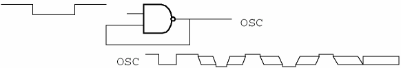
Figure 16-10 Cumulative ambiguity hazard example three.
Due to the accumulation of ambiguity in the loop, the output signal will eventually become X, because the ambiguities of the rising and falling edges overlap. However, in the hardware implementation of this circuit, a continuous phase shift with respect to absolute time is what will actually occur (assuming normal deviations of the rise and fall delays from the nominal values).
Reconvergence hazard
PSpice A/D recognizes situations where signals having a common origin reconverge on the inputs of a single device. In Figure 16-11, the relative timing relationship between the two paths (U2, U3) is important.
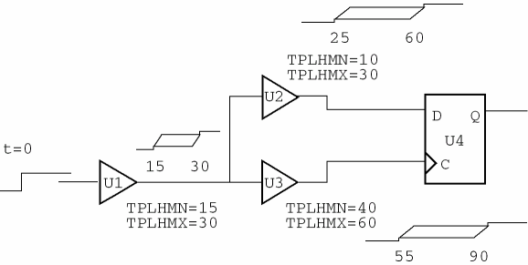
Figure 16-11 Reconvergence hazard example one.
Given the delay values shown, it is impossible for the clock to change before the data input, since the MAX delay of the U2 path is smaller than the MIN delay of the U3 path. In other words, the overlap of the two ambiguity regions could not actually occur.
PSpice A/D recognizes this type of situation and does not produce the overly pessimistic result of latching an X state into the Q-output of U4. This factors out the 15 nsec of common ambiguity attributed to U1 from the U2 and U3 signals (see Figure 16-12).
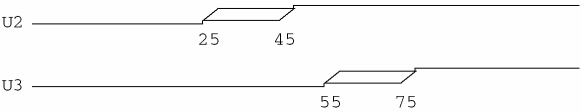
Figure 16-12 Reconvergence hazard example two.
The result in Figure 16-12 does not represent what is actually propagated at U2 and U3, but is a computation to determine that U2 must be stable at the earliest time U3 might change. This is why an X level should not be latched.
In the event that discounting the common ambiguity does not preclude latching the X (or, in the case of simple gates, predicting a glitch), the situation is called a reconvergence hazard. This is the same as a convergence hazard with the conflicting signal ambiguities having a common origin.
To use digital worst-case simulation effectively, find the areas of the circuit where signal timing is most critical and use constraint checkers where appropriate. These devices identify specific timing violations, taking into account the actual signal ambiguities (resulting from the elements’ MIN/MAX delay characteristics). See the PSpice A/D Reference Guide for more information about digital primitives.
The most common areas of concern include:
- data/clock signal relationships
- clock pulse-widths
- bus arbitration timing
Signal ambiguities that converge (or reconverge) on wired nets or buses with multiple drivers may also produce hazards in a manner similar to the behavior of logic gates. In such cases, PSpice A/D factors out any common ambiguity before reporting the existence of a hazard condition.
The use of constraint checkers to validate signal behavior and interaction in these areas of your design identifies timing problems early in the design process. Otherwise, a timing-related failure is only identifiable when the circuit does not produce the expected simulation results. See Methodology for information on digital worst-case timing simulation methodology.
Glitch suppression due to inertial delay
Signal propagation through digital primitives is performed by the simulator subject to constraints such as the primitive’s function, delay parameter values, and the frequency of the applied stimulus. These constraints are applied both in the context of a normal, well-behaved stimulus, and a stimulus that represents timing hazards.
Timing hazards may not necessarily result in the prediction of an X or glitch output from a primitive; these are due to the delay characteristics of the primitive, which PSpice A/D models using the concept of inertial delay.
A device presented with a combination of rising and falling input transitions (assuming no other dominant inputs) produces a glitch due to the uncertainty of the arrival times of the transitions (see Figure 16-13).
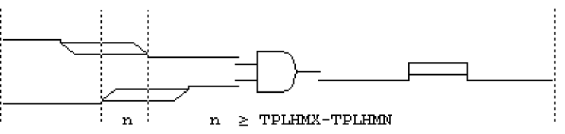
Figure 16-13 Glitch suppression example one.
However, when the duration of the conflicting input stimulus is less than the inertial delay of the device, the X result is automatically suppressed by the simulator because it would be overly pessimistic (see Figure 16-14).
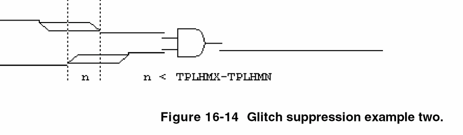
In the analysis of reconvergent fanout cases (where common ambiguity is recognized), it is possible that conflicting signal ambiguities may still overlap at the inputs to a primitive, even after factoring out the commonality. In such cases, where the amount of overlap is less than the inertial delay of the device, the prediction of a glitch is also suppressed by the simulator (see Figure 16-15).
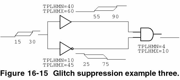
In this case, factoring out the 15nsec common ambiguity still results in a 5nsec overlap of conflicting states. The glitch is suppressed, however, because 5nsec is less than TPLHMX-TPLHMN (the computed inertial delay value of the AND gate, 6nsec).
Methodology
Combining component tolerances and the circuit design’s functional response to a specific stimulus presents a challenge. You must make sure that all the finished circuits will operate properly. Well-designed systems have a high degree of immunity from the effects of varying combinations of individual component tolerances.
Digital worst-case timing simulation can help identify design problems, depending upon the nature of the stimulus applied to the design. You can use the simulation of signal propagation through the network to observe the timing relationships among various devices and make adjustments to the design.
Digital worst-case timing simulation does not yield such results without an applied stimulus; it is not a static timing analysis tool. The level of confidence that you establish for your design’s timing-dependent characteristics is directly a function of the applied stimulus.
Generally, the most productive way to define a stimulus is to use functional testing: a stimulus designed to operate the design in a normal manner, exercising all of the important features in combination with a practical set of data. For example, if you were designing a digital ADDER circuit, you would probably want to ensure that no timing race conditions existed in the carry logic.
Your timing simulation methodology should include these key steps:
- Accurate specification of device delay characteristics.
- Functional specification of circuit behavior, including all "don’t care" states or conditions.
- A set of stimuli designed to verify the operation of all functions of the design.
One common design verification strategy is stepwise identification of the sections of the design that are to be exercised by particular subsets of the stimulus, followed by verification of the response against the functional specification.
Complete this phase using normal (not digital worst-case) simulation, with typical delays selected for the elements. The crucial metric here is the state response of the design. Note that (with rare exception) this response consists of defined states and does not include X’s.
The second phase of design verification is to use digital worst-case simulation, reapplying the functionally correct stimulus, and comparing the resulting state response to that obtained during normal simulation. For example, in the case of a convergence or reconvergence hazard, look for conflicting rise/fall inputs. In the case of cumulative ambiguity, look for successive ambiguity regions merging within two edges forming a pulse. Investigate differences at primary observation points (such as circuit outputs and internal state variables)—particularly those due to X states (such as critical hazards)—to determine their cause.
Starting at those points, use the waveform analyzer and the circuit schematic to trace back through the network. Continue until you find the reason for the hazard.
After you identify the appropriate paths and know the relative timing of the paths, you can do either of the following:
- Modify the stimulus (in the case of a simple convergence hazard) to rearrange the relative timing of the signals involved.
Modifying the stimulus is not generally effective for reconvergent hazards, because the problem is between the source of the reconvergent fanout and the location of the hazard. In this case, discounting the common ambiguity did not preclude the hazard. - Change one or both of the path delays to rearrange the relative timing, by adding or removing logic, or by substituting component types with components that have different delay characteristics.
In the case of the cumulative ambiguity hazard, the most likely solution is to shorten the path involved. You can do this in either of two ways:
- Add a synchronization point to the logic, such as a flip-flop—or gating the questionable signal with a clock (having well-controlled ambiguity)—before its ambiguity can grow to unmanageable duration.
- Substitute faster components in the path, so that the buildup of ambiguity happens more slowly.
View the next document: 17 - Waveform Analysis
If you have any questions or comments about the OrCAD X platform, click on the link below.
Contact Us