11 - Sample Circuits
The PSpice Simulink Co-Simulation demonstrations and example files for:
- Capture are available at:
<installation_directory>\tools\pspice\capture_samples\CoSimulationDemos\PSpiceCoSim - Design Entry HDL are available at:
<installation_directory>\tools\pspice\concept_samples\CoSimulationDemos\PSpiceCoSim
This section explains some circuits, which explain the use of the PSpice Simulink Co-Simulation interface.
- RLC Circuit
- RC Circuit
- Nonlinear Load (NLLOAD)
- PLL Model
- Switched Reluctance Motor Control
- Switching Power Supply
- DC Motor Control System
RLC Circuit
Use a simple RLC circuit (RLCCir), as shown in the following figure to create the schematic diagram.
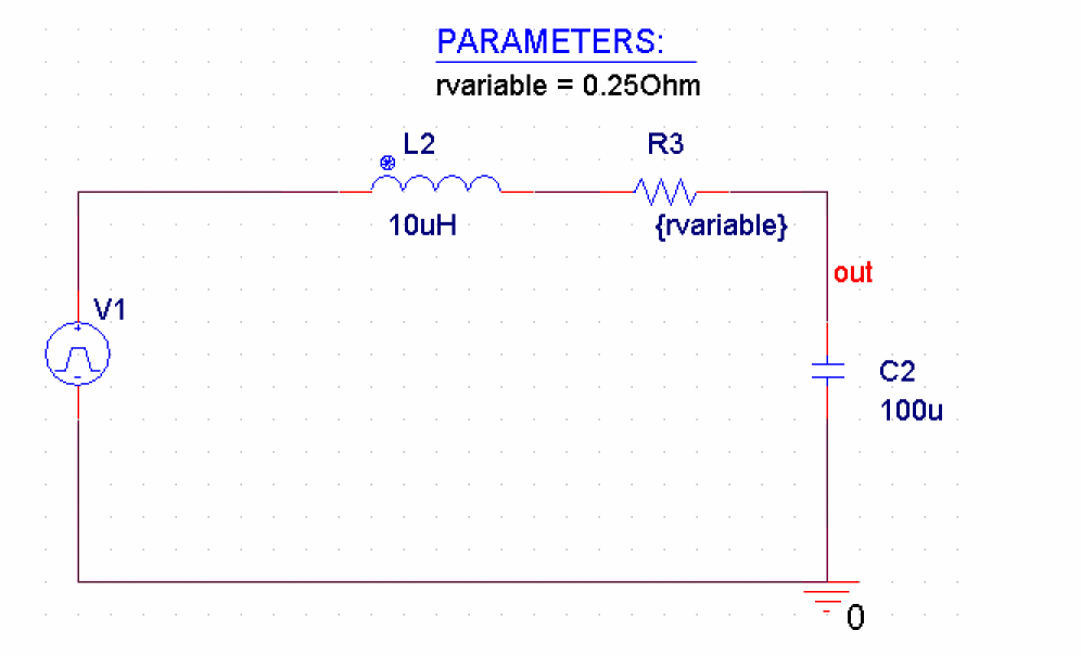
Figure A-1 RLC Circuit
Simulink Block Diagram
Figure A-2 shows the Simulink block diagram (RLC.slx).
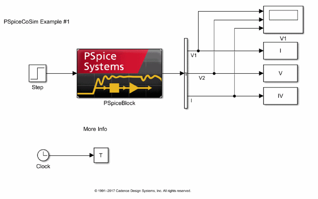
Figure A-2 Simulink block diagram
The following table list the various PSpice block parameters.
| Parameter | Description |
|---|---|
| Capture project file | RLC.opj |
| PSpice circuit file | tran.cir |
| Input Source | V1 Input data from Simulink as a voltage value, using the voltage source V1 in the circuit. |
| Outputs | I(C2:1) V(OUT) W(R3) |
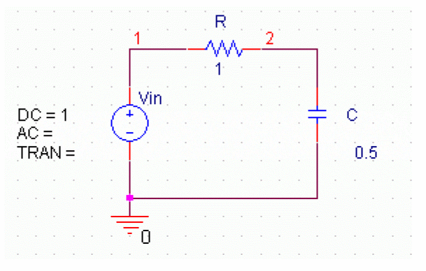
RC Circuit
Use a simple RC circuit (RCCIR), as shown in the following figure to create the schematic diagram.
Simulink Block Diagram
The following figure shows the Simulink block diagram, RCMDL_SLPS.slx.
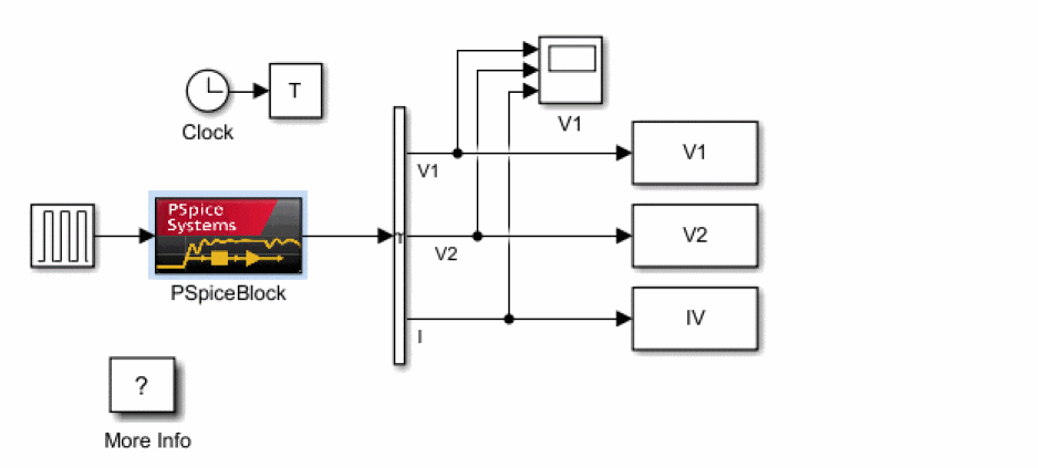
Figure A-3 Simulink block diagram
The following table list the various PSpice block parameters.
| Parameter | Description |
|---|---|
| Capture project file | RCCIR.opj |
| PSpice circuit file | tran.cir |
| Input source | Vin Input data from Simulink as a voltage value, using the voltage source Vin in the circuit. |
| Outputs | I(R:1) V(C:2) W(R) For Simulink, the current value passing through the resistor R, the output voltage at node 2, and the power dissipation through resistor R. |
| Data saving option | None In order not to save analyzed data in SLPS and to speed up analysis, select None. |
| ITL4 Max | 10 Convergence errors rarely occur because this is a linear circuit, so set it to the default value of 10 times. |
Analysis Settings and Results
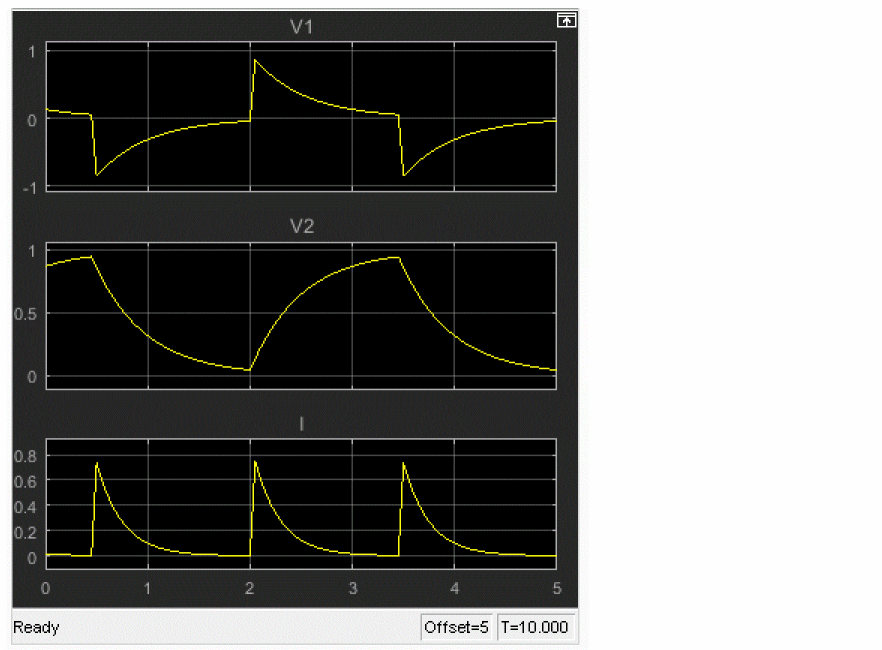
In the Simulink analysis settings, analysis is set up with a step size of 0.1 seconds, from 0 to 10 seconds. Following results are seen when you run the simulation from the Simulink window.
Nonlinear Load (NLLOAD)
In this example, you will simulate the state where the values of devices in the circuit are controlled by Simulink and the load connected to the circuit is nonlinear.
Schematic
The electric circuit is roughly divided into two parts, an amplifier and a load connected to the output of the amplifier, as shown in the following figure. The load resistance is determined by Simulink.
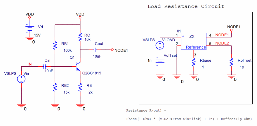
Figure A-4 Nonlinear load circuit
The voltage control impedance ZX/anl_misc.olb is used as the load resistance of the circuit. The output impedance of this device is determined by the following formula:
![]()
where:
 :Impedance between output pins
 :Reference impedance (connected to Reference pin)
 :Control voltage
In the circuit, a VSLPS voltage source, which adds a 1nV offset, is connected between the ZX control voltage pins, and a 1![]() reference resistor is inserted between the Reference pin and ground. A 1
reference resistor is inserted between the Reference pin and ground. A 1![]() load impedance offset resistor is connected between NODE2 and ground, and NODE1 is connected to the output of the amplifier circuit.
load impedance offset resistor is connected between NODE2 and ground, and NODE1 is connected to the output of the amplifier circuit.
Therefore, the load impedance in respect to the amplifier circuit is given by the following formula:
![]()
Simulink Model
The following figure shows the Simulink block diagram, NLLOAD_SLPS.slx.
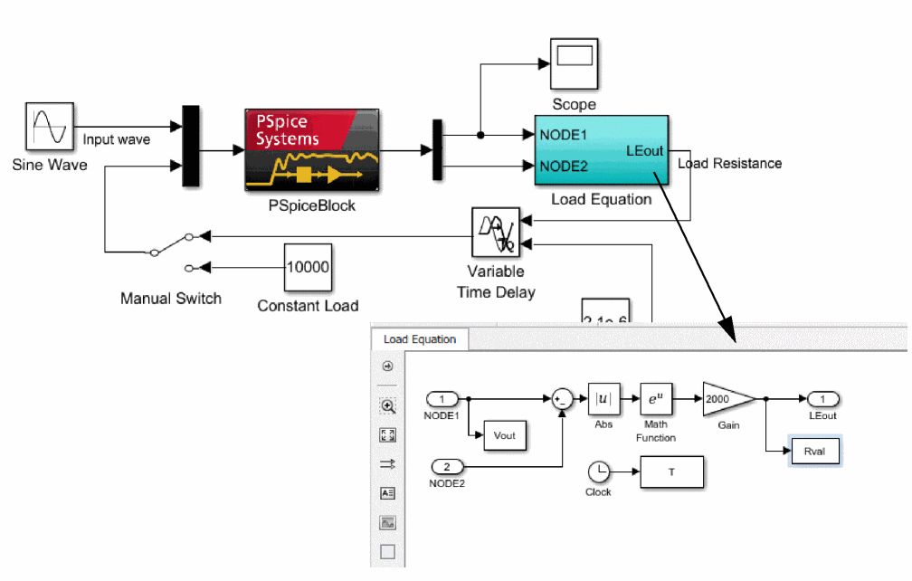
The voltage values of NODE1 and NODE2 are taken as output from SLPS. The load resistance characteristic is determined by the hierarchical block "Load Equation". The resistance value is returned to SLPS and is determined as follows:
![]()
The resistance value ![]() is an exponential function of the voltage differential between NODE1 and NODE2.
is an exponential function of the voltage differential between NODE1 and NODE2.
In this model, when the SLPS block is inserted in the feedback loop, a delay of one cycle step of Simulink occurs between the feedback loop's input (SLPS block's input) and output (SLPS block's output). Therefore, to obtain high-precision results, you must force Simulink to take small time steps.
Results
The following figure shows the output voltage (V (NODE1)) waveform in the upper part and the waveform of the resistance value in the lower part. To plot the resistance value, you need to add another SCOPE at the Load Resistance node in the block diagram.
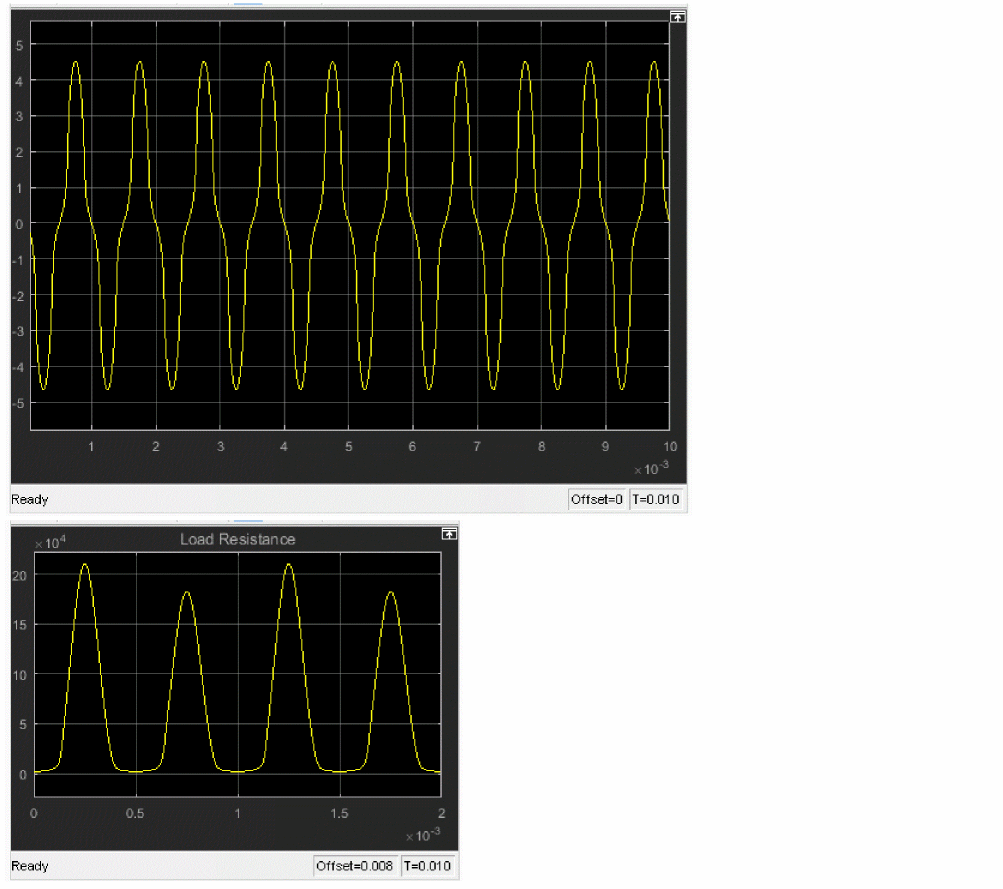
The output voltage vs. resistance characteristic is shown in the following figure and can be plotted by running the nlloadplt.m file.
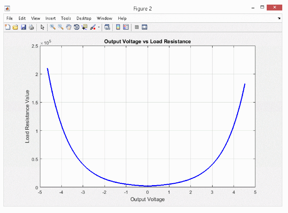
Figure A-5 Output voltage vs. resistance characteristics
You can confirm that the load value changes with time, and, as a result, the output voltage waveform is distorted.
This example shows a nonlinear load, but it can be applied to load fluctuation of a motor or counter EMF.
PLL Model
A Phase Locked Loop (PLL) circuit can halve transmitter output that is synchronized with the input signal and, as a result, expands usability to digital circuit blocks, mobile communications, and so on.
PLL Composition
PLL is comprised of the following three modules:
- Phase comparator
- Loop filter
- VCO
The phase comparator detects the phase difference between two signals, and outputs that difference. As shown in the Figure, A-6 it detects the phase difference between the input signal to the PLL, and the feedback PLL output signal.
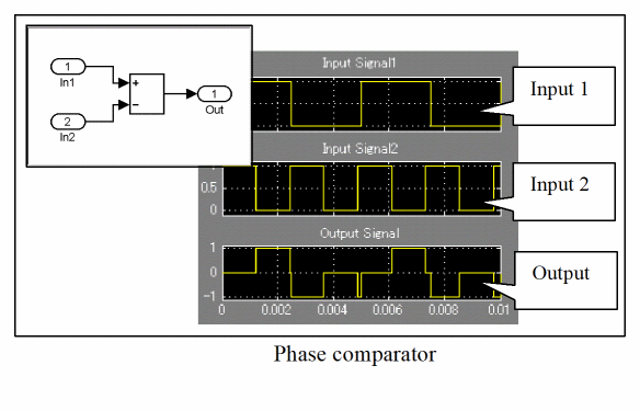
Figure A-6 Phase comparator
The PLL input/output waveform to be designed here is assumed to be a pulse waveform, so it is given by a simple adder, as shown in the figure. In reality, the output value offset is adjusted by the characteristics of the loop filter and VCO being used.
The loop filter eliminates AC components from the phase comparator output and creates a VCO control signal for the next stage. A loop filter is an Low Pass Filter (LPF), and a transmission function block is used in Simulink. In Figure A-7, the frequency characteristic, when fc=10Hz, can be checked using the freqs function of MATLAB.
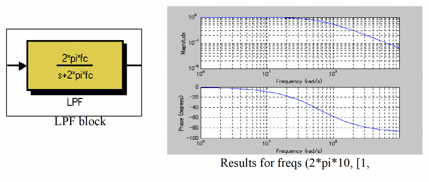
Figure A-7 Frequency characteristic at fc=10Hz
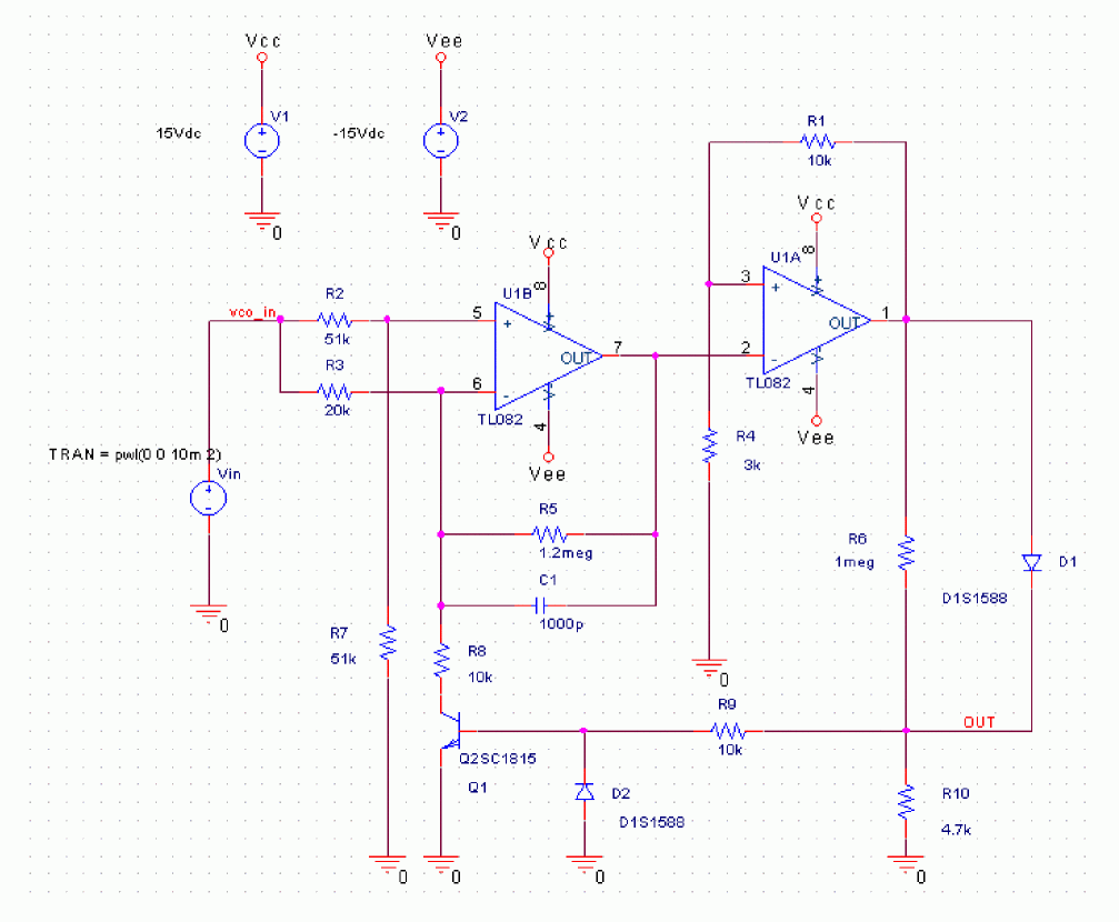
A Voltage Controlled Oscillator (VCO) is an oscillating circuit where oscillation frequency varies with control voltage. In the end, the output of this VCO becomes the output of the PLL. Therefore, the VCO control voltage is controlled so that the oscillation frequency is synchronized with the PLL input signal. The VCO electrical circuit described in the Capture project file VCO.opj is shown in the following figure.
The simulation results using PSpice are shown in Figure A-8:
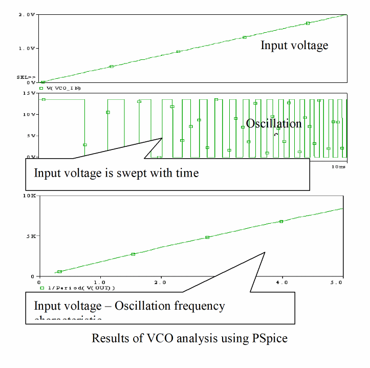
Figure A-8 Simulation result for VCO analysis using PSpice
You can see that the oscillation frequency is about 1.8 KHz at an input voltage of 1V, and it increases almost linearly along with an increase in the input voltage.
PLL model incorporating VCO electric circuit
The Simulink PLL model is shown in the following figure.
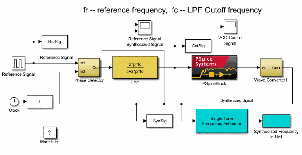
In this section, an electrical circuit is incorporated by SLPS in VCO only, and the entire PLL operation is checked. If an electrical circuit is incorporated in a loop filter to phase comparator, delays of elements used in the circuit and the effects of the circuit’s time constant can also be confirmed.
The simulation results for VCO are shown in the following figures.
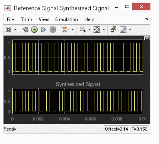
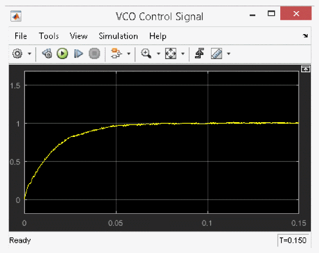
From the VCO control signal, it can be confirmed that the oscillation frequency is locked after 70ms.
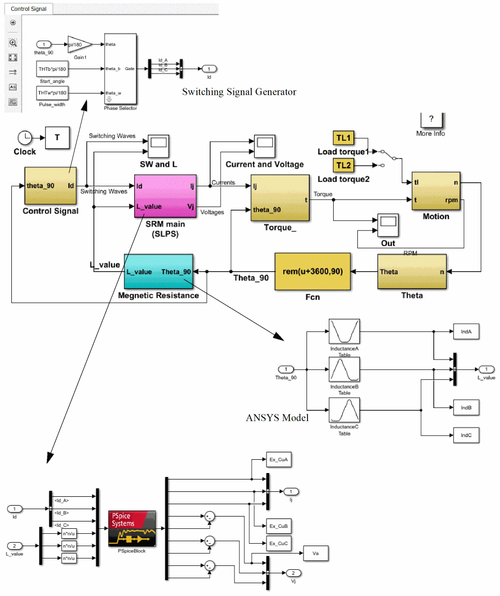
Switched Reluctance Motor Control
When designing a motor control system, you need to understand the characteristics of the entire system, such as torque determined by motor dimension, the electric circuit including motor inductance, and switching device, and position control associated with rotor rotation.
Analyzing magnetic field using finite element method
With ANSYS, a general-purpose finite element analysis program, you analyze electromagnetic field of the motor form and obtain the inductance value to model a motor.
The switched reluctance motor (SRM) used here as an analysis example employs a 3-phase excitation motor, with 6 stator poles and 4 rotor poles, as shown in Figure A-9.
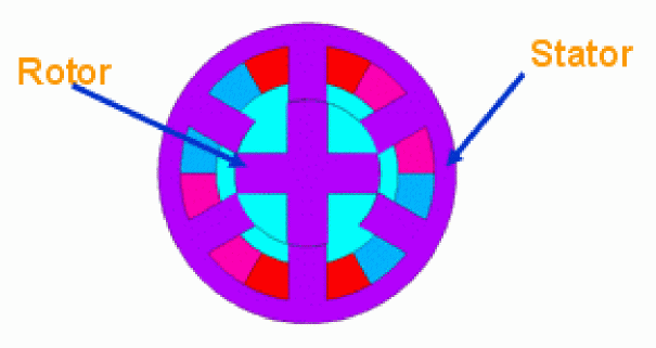
Figure A-9 SRM Model
The SRM can obtain torque using only the magnetic force between rotors and stators. Therefore, if L be the excitation coil inductance, i the current, and W the magnetic energy, the torque T can be expressed using the following formula:
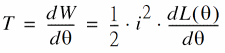
Therefore, torque is derived from changes in inductance. The inductance of the excitation coil to drive the motor varies with the rotation angle of the rotor. You can obtain the inductance value for each angle by performing magnetic field analysis of the motor.
The analysis result and the inductance related to rotor angle is shown by Figure A-10:
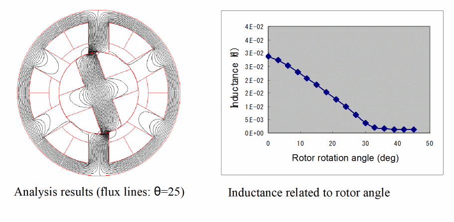
Figure A-10 Analysis result and rotor angle
Modeling of electric circuit using PSpice
Figure A-11 shows the electrical circuit model.
Figure A-11 Electrical circuit model
The inductor model placed in the circuit indicates motor inductance components. The inductor value can be determined externally using modeling techniques that separate electrical characteristics and magnetic circuits. During analysis, analysis results from ANSYS are referenced by Simulink, and the inductance value determined by the rotor position is passed as a parameter. The gate signal of the switching transistor is also provided from Simulink, the current value passing through the inductance is monitored, and its value is returned to the outside.
Simulink model
The entire motor control model created with Simulink is shown in the following figure.
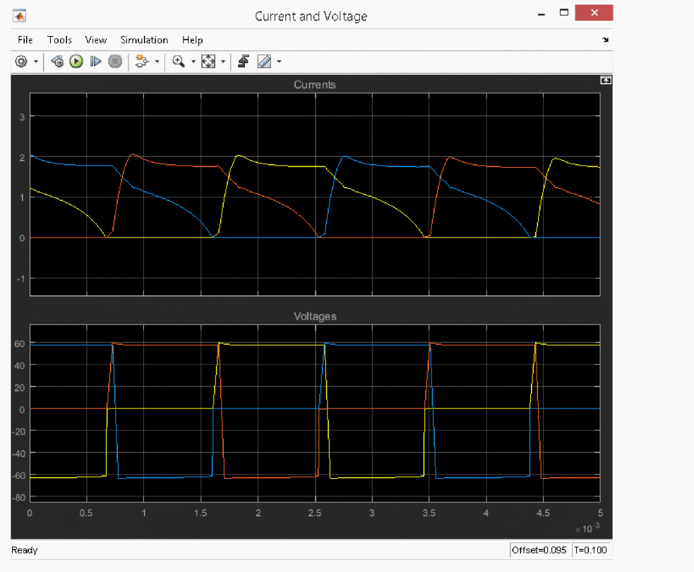
The results for current and voltage values for each phase is shown in the following figure.
The torque and rotation speed results are shown in the following figure.
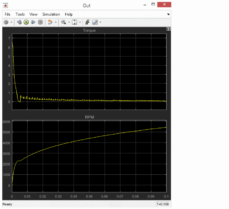
The number of rotations varies with load torque, motor dimensions, switching device and switching waveform. These effects can also be simulated.
Switching Power Supply
Power electronics circuits, such as switching power supplies and motor control, might have both electric circuits that switch a large current and high voltage in a short time using a power device, and control circuits with ICs. If you attempt to model an entire circuit of this type using an electric circuit simulator such as SPICE, you must express all of the control parts with the electric device level. In this case, the entire circuit becomes complex, so you may have to spend a lot of time not for verification but for other tasks at the initial stage of design. As the number of devices increases, convergence errors are likely to occur. As a result, it may take longer to analyze data or, in the worst-case scenario, analysis might stop before it is complete.
On the other hand, if the entire circuit is simulated with the system simulator MATLAB/Simulink, it is easier to express the control algorithm in numerical formulas, but it is difficult to accurately express the rise or fall characteristics of the switching device, and the electrical characteristics of inductors and transformers because it does not have a library of devices.
Electric circuit design using PSpice
Figure A-12 shows the circuit diagram with the forward converter inserted:
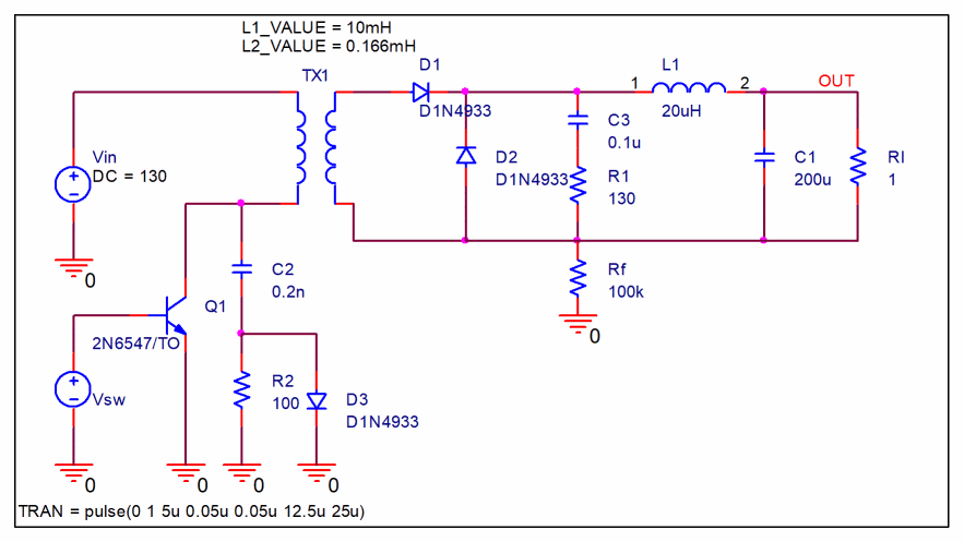
Figure A-12 Circuit with forward converter
The conditions for this circuit are as follows:
- Rated input voltage:130V
- Output voltage:10V
- Output current: 10A
Here, find the optimal voltage of the snubber circuit's capacitor connected to Q1 in order to minimize power loss due to switching.
Figure A-13 shows the VCE waveform of Q1 when the value of C2 is varied from 0.1n to 1.0n using the PSpice function of parametric analysis.
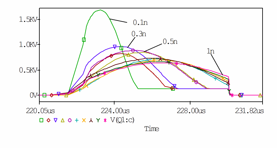
Figure A-13 VCE waveform of Q1
From these results, you can see that the optimal value is approximately 0.5nF where power loss is limited and VCE takes the smallest value during switching.
When 0.5nF is applied to C2, the output current, voltage and VCE waveforms, as shown in the Figure A-14, appear:
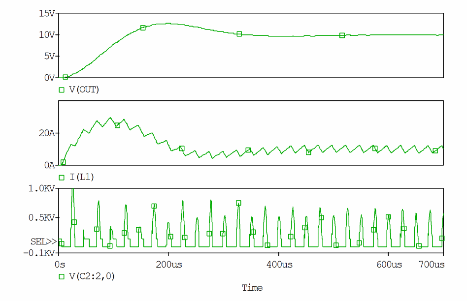
Figure A-14 Voltage and VCE waveform
To specify load from Simulink, use a variable impedance ZX instead of the load resistor R1, thereby making it possible to determine the resistance value using Vload. The circuit is shown in Figure A-15.
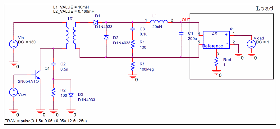
Figure A-15 Circuit using variable impedance
Control system design using Simulink
Using MATLAB/Simulink, design a PWM controller by placing an SLPS block as shown in Figure A-16.
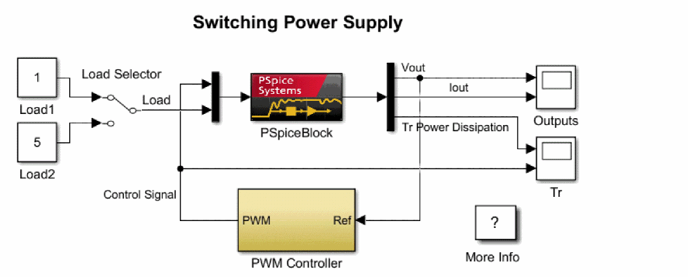
Figure A-16 PWM Controller design
Assign the previous circuit diagram to the SLPS block, designate the output voltage ![]() and output current
and output current ![]() , and the power dissipation of the switched transistor
, and the power dissipation of the switched transistor ![]() Power Dissipation. In the PWL control model, the PI controlled output voltage is compared with the reference value Reference, and then with a triangle wave, to create a PWM signal.
Power Dissipation. In the PWL control model, the PI controlled output voltage is compared with the reference value Reference, and then with a triangle wave, to create a PWM signal.
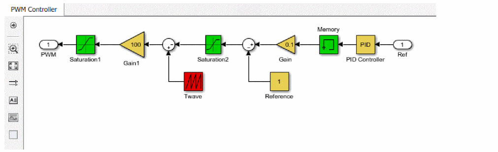
Figure A-17 PWL Controller
In the PWL control model, the PI controlled output voltage is compared with the reference value, Reference, and then with a triangle wave to create a PWM signal.
Results
Set up analyses in Simulink is as follows:
- Stop time: 1e-3 sec
- Solver type: Fixed step
- Solver: ode5
- Step size: 1e-6 sec
Figure A-18, Figure A-19, and Figure A-20 show simulation results when the load resistance is set to ![]() .
.
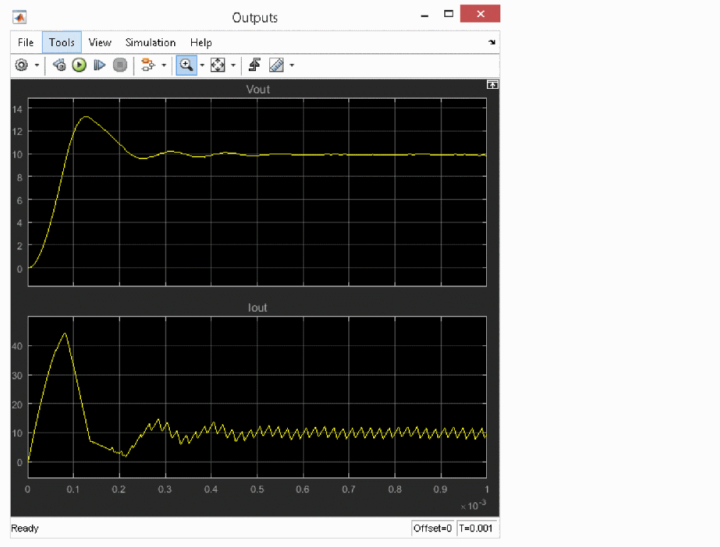
Figure A-18 Output voltage and current
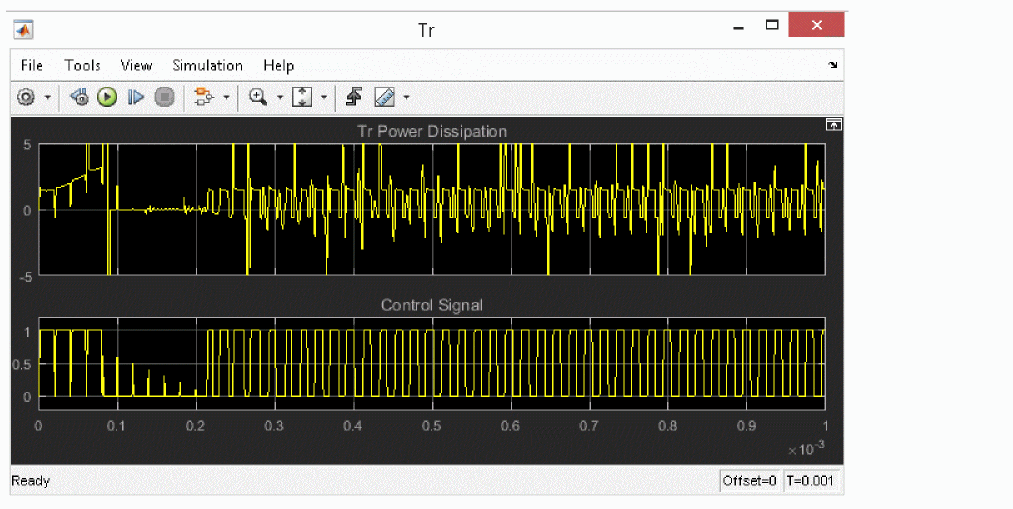
Figure A-19 Transistor power dissipation and switching signal waveform
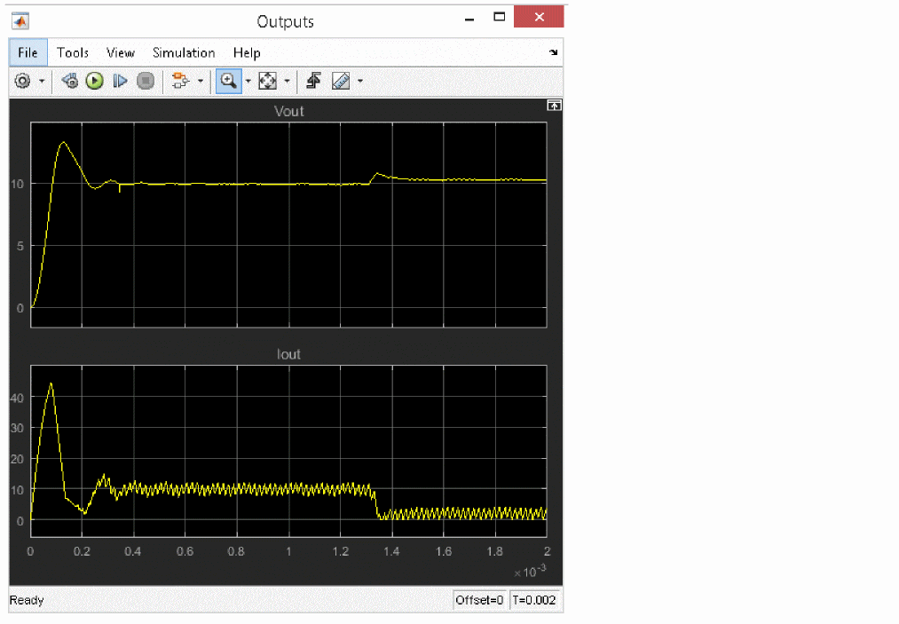
Figure A-20 Changing load resistance from 1 to 5![]() near 1.3mS
near 1.3mS
From the results, you can see that output stabilizes at about 0.4mS after starting the simulation, and it changes along with the fluctuations in load.
In this design example, PSpice has been used for electrical circuits, and the Simulink design environment for control. Electrical circuits have been used for the parts where electrical characteristics (like element delay) have an effect and those which are difficult to express in formulas. To design the basic circuit, PSpice has been used. To design the control system which drives the circuit, a Simulink model which is flexible in expressing numerical formulas has been used. Finally, both models have been combined using SLPS, with which the entire system has been simulated while taking electrical characteristics into consideration.
DC Motor Control System
Due to the trade-off between simulation speed and result accuracy, it is not an efficient method to use highly accurate models at the first stage of designing, as the simulation speed will be very slow. It is recommended to use proper models for each stage of designing process. You may find that proper modeling makes optimizing the system parameters easier.
Outline of DC motor control system
Figure A-21 shows the diagram of a DC motor control system.
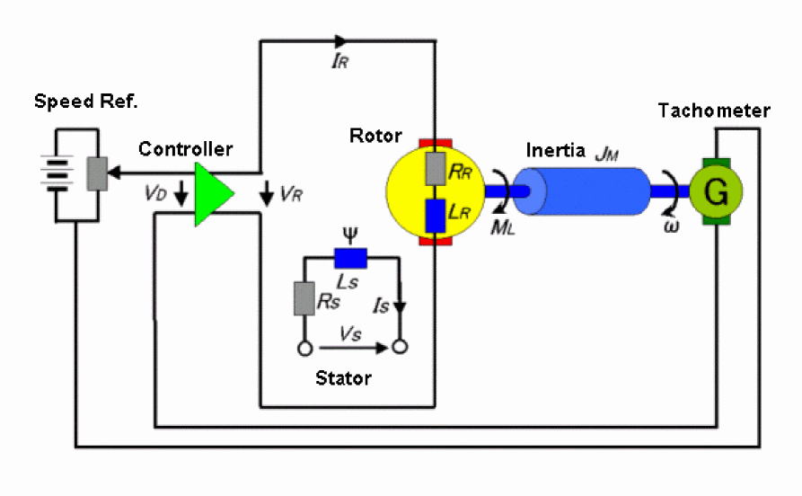
Figure A-21 DC motor control system
This diagram consists of a stator or field winding which produces a constant magnetic flux for excitation. This winding is modeled by inductance Ls and resistance Rs. When voltage Vs is applied to the stator winding, current Is flows which produces flux. The rotor winding is also modeled by its inductance LR and resistance RR. When voltage VR is applied to the rotor winding, current IR flows. VR is the output of a controller which is driven by a differential input voltage VD. The signal flow is from VD to VR but not in the reverse direction. As a result, the armature reaction between rotor and stator is neglected.
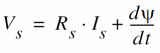
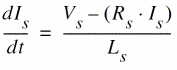
First, write the mesh equation for the stator winding:
In general, the magnetic flux ![]() is a nonlinear function of the stator current
is a nonlinear function of the stator current ![]() . For simplicity, assume
. For simplicity, assume ![]() to be a linear function of
to be a linear function of ![]() :
:
![]()
As a result,
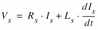
or
For the mesh equation of the rotor winding:
or
For the moments on the rotor shaft, you can write the balance equation:
![]()
where,
![]()
and
![]()
![]() is the rotor driving torque, which is a linear function of excitation flux
is the rotor driving torque, which is a linear function of excitation flux ![]() and rotor current
and rotor current ![]() multiplied by constant
multiplied by constant ![]() .
. ![]() is the given load moment and
is the given load moment and ![]() is the internal friction moment of the motor which is assumed to be a linear function of angular velocity
is the internal friction moment of the motor which is assumed to be a linear function of angular velocity ![]() multiplied by constant
multiplied by constant ![]() .
. ![]() is the moment of inertia of all rotating masses mechanically connected to the rotor.
is the moment of inertia of all rotating masses mechanically connected to the rotor.
The controller is driven by the voltage difference ![]() between the speed potentiometer voltage, which sets the nominal angular velocity
between the speed potentiometer voltage, which sets the nominal angular velocity ![]() and the tachometer voltage, which is proportional to angular velocity
and the tachometer voltage, which is proportional to angular velocity ![]() . You can write
. You can write ![]() as the difference between the angular velocities multiplied by constant
as the difference between the angular velocities multiplied by constant ![]() :
:
![]()
For the controller, use a PI characteristic which is described by:
![]()
Simulink Model
First, model the whole system in Simulink, as shown in figure A-22.
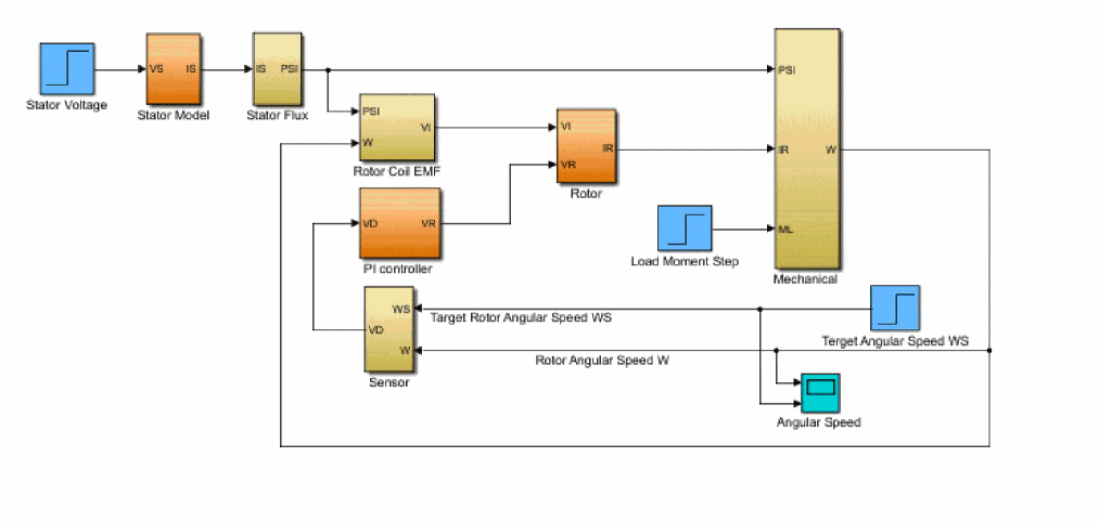
Figure A-22 System model
Specify the parameters:
![]() = 0.50
= 0.50
![]() = 0.50
= 0.50
![]() = 0.10; % N*m*s
= 0.10; % N*m*s
![]() = 0.01; % V*s
= 0.01; % V*s
![]() = 606.0; % 1/s
= 606.0; % 1/s
![]() = 100.0
= 100.0
![]() = 0.10; % H = V*s/A
= 0.10; % H = V*s/A
![]() = 10.0; % H = V*s/A
= 10.0; % H = V*s/A
![]() = 0.50; % Ohm = V/A
= 0.50; % Ohm = V/A
![]() = 500.0; % Ohm = V/A
= 500.0; % Ohm = V/A
![]() = 1.0; %
= 1.0; % ![]()
Figure A-23 shows the plots for the angular velocities ![]() ) and
) and ![]() .
.
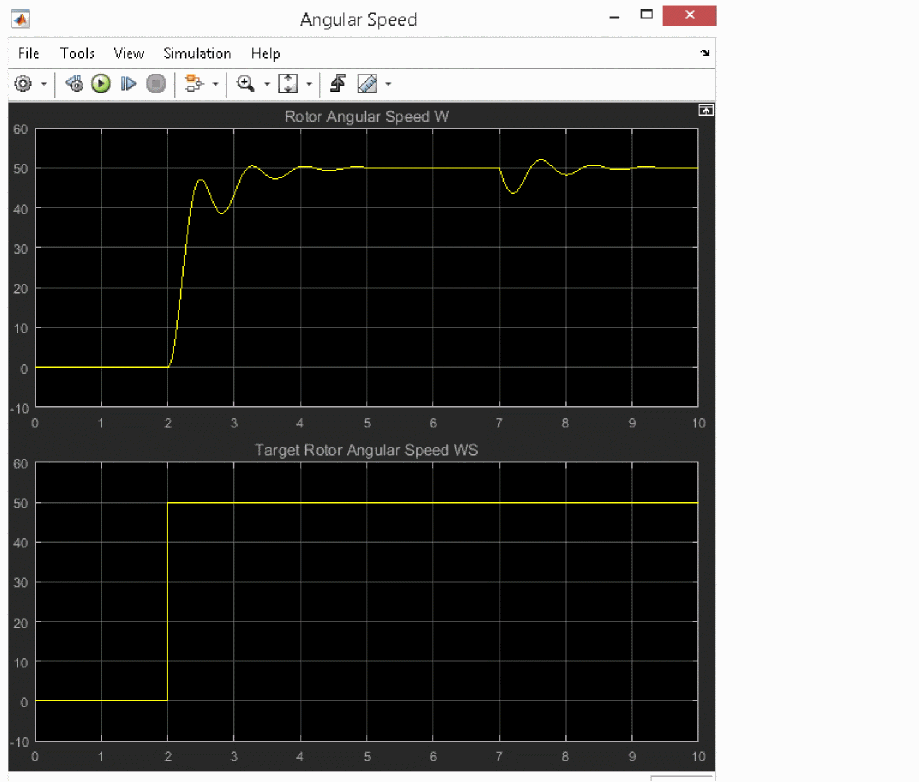
Figure A-23 Plots for the angular velocities ![]() ) and
) and ![]()
The stator voltage ![]() is switched on at time t=1s.
is switched on at time t=1s. ![]() is set to 50 rad/s at 2s and the rotor starts to turn. At about t=6s,
is set to 50 rad/s at 2s and the rotor starts to turn. At about t=6s, ![]() reaches the steady state of 50 rad/s.
reaches the steady state of 50 rad/s.
At t=7s, a load moment of 50 Nm is applied and the rotor speed reduces to 43.6 rad/s. Therefore, the controller increases VR and the new steady state of ![]() =50 rad/s is reached again at about t=10s.
=50 rad/s is reached again at about t=10s.
Simulink-PSpice Model (Ideal Opamp)
With the results of the Simulink model available for reference, you can now replace some of the Simulink blocks to PSpice circuits. Figure A-24 shows the system block diagram.
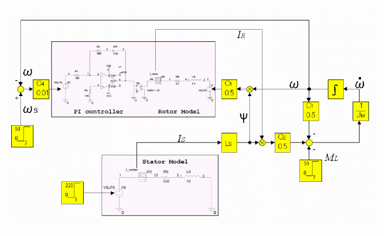
Figure A-24 Ideal Opamp system block diagram
Figure A-25 shows the Simulink model, which includes PSpice circuits using SLPS.
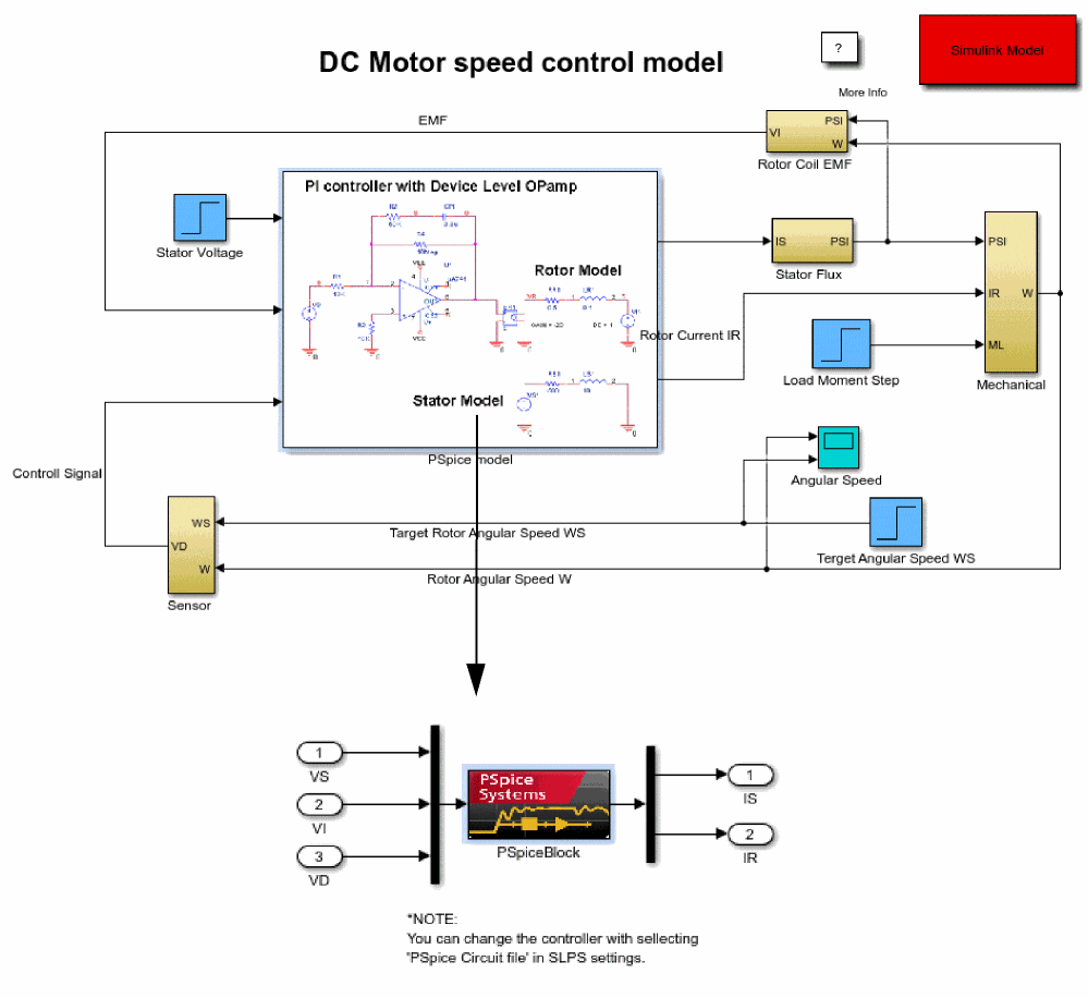
Figure A-25 Simulink model including PSpice circuits
Figure A-26 shows the stator circuit.
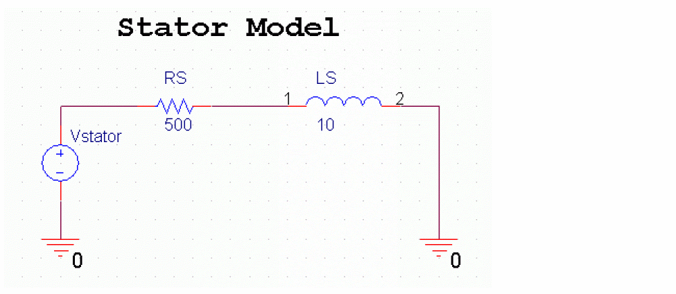
Figure A-26 Stator model
Figure A-27 shows the rotor circuit:
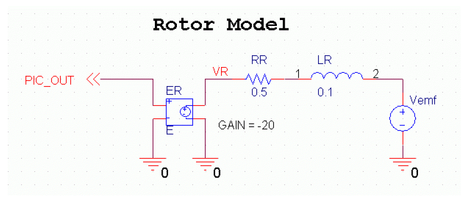
Figure A-27 Rotor model
Figure A-28 shows the PI controller circuit:
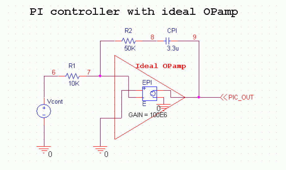
Figure A-28 PI controller circuit
Circuit elements ![]() ,
, ![]() ,
, ![]() and
and ![]() ,
, ![]() ,
, ![]() implement the equation for
implement the equation for ![]() and
and ![]() . For the operational amplifier(Opamp) in the PI controller, first use an ideal model with very high open-loop gain, infinite input resistance, zero output resistance, zero input offset voltage, zero input offset and bias current, and no output voltage saturation. This behavior is easily modeled in SPICE by a linear voltage-controlled voltage source. The PI controller output voltage V(9)(PIC_OUT) is given by the equation.
. For the operational amplifier(Opamp) in the PI controller, first use an ideal model with very high open-loop gain, infinite input resistance, zero output resistance, zero input offset voltage, zero input offset and bias current, and no output voltage saturation. This behavior is easily modeled in SPICE by a linear voltage-controlled voltage source. The PI controller output voltage V(9)(PIC_OUT) is given by the equation.
with the factors,
![]()
The corner frequency ![]() where the I and P characteristics meet is:
where the I and P characteristics meet is:
![]()
Voltage ![]() controls the voltage-controlled voltage source
controls the voltage-controlled voltage source ![]() , which has a gain value of -20. Therefore, you obtain:
, which has a gain value of -20. Therefore, you obtain:
![]()
Comparing this equation to the one for ![]() in the pure Simulink model, you will observe that both are identical because of constant values
in the pure Simulink model, you will observe that both are identical because of constant values ![]() =606 and
=606 and ![]() =100. The PSpice controller circuit, therefore, implements the same equation
=100. The PSpice controller circuit, therefore, implements the same equation ![]() for as in subsystem PI-CONTROLLER in Simulink model.
for as in subsystem PI-CONTROLLER in Simulink model.
Simulink-PSpice Model Result (Ideal Opamp)
Figure A-29 shows the simulation results, ![]() and
and ![]() ) for PI controller with ideal Opamp:
) for PI controller with ideal Opamp:
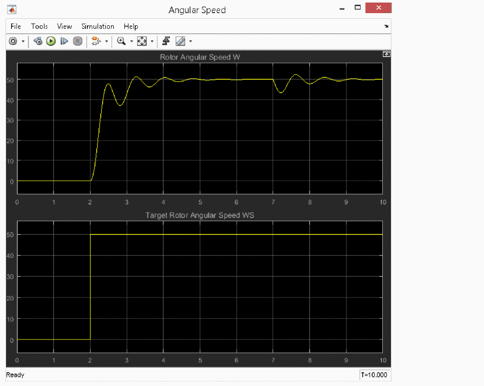
Figure A-29 Simulation results for PI controller with ideal Opamp
Simulink-PSpice Model (Device Opamp)
You can now replace the ideal Opamp model in the PI controller with a device-level model of a standard µA741 Opamp, as shown in Figure A-30:
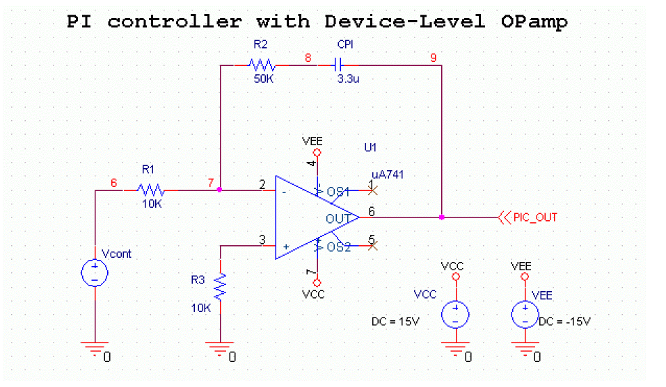
Figure A-30 PI controller with uA741
Figure A-31 shows the simulation results, ![]() for PI controller with µA741:
for PI controller with µA741:
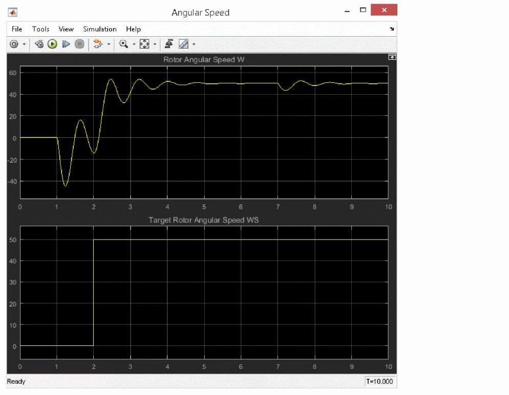
Figure A-31 Simulations results for PI controller with uA741
After the excitation is turned on at 1s, the motor starts to turn in the opposite direction., The device-level model behaves differently from the ideal Opamp model used in the controller. This is because the Opamp output goes into saturation as a result of the input offset voltage and the very high open-loop gain at DC operating point calculation at t=0.
To avoid the offset problem, ![]() resister
resister ![]() was put in the feedback loop to limit the DC gain to 1000, as shown in Figure A-32.
was put in the feedback loop to limit the DC gain to 1000, as shown in Figure A-32.
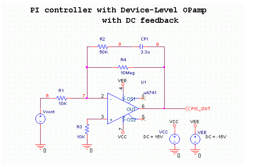
Figure A-32 PI controller circuit with DC feedback
Figure A-33 shows the result of the simulation for ![]() for PI controller with
for PI controller with ![]() :
:

Figure A-33 Simulation results for PI controller with DC feedback
Because the Opamp output offset voltage is reduced and the initial transient in the opposite direction is also reduced. A negative effect of the reduced DC gain is that the steady-state response of ![]() differs slightly from 50 rad/s.
differs slightly from 50 rad/s.
If you have any questions or comments about the OrCAD X platform, click on the link below.
Contact Us