Common DFM “Gotchas”
Image credit: Cadence
We all cherish the day our imaginary boards become real-life hardware. Wait. We all dread the day… It is natural to the point of being predictable how it works out that we execute a major project and the next link of the chain adds on right from there. Typically, the scenario is that we met a revised schedule but clamor to catch up to the initial timeline. That one was from before me made contact with reality. So it stands to reason that we want to hit the ground running with our data hand-off. In order to prime the pump, it’s a good idea to get out in front of these typical DFM callbacks from your favorite vendor.
Via Plating
The request to reduce the minimum required copper thickness in the via barrel could be considered automatic in some situations. When the job gets more complex, the copper thickness of the conductor layers becomes a process variable. Narrow air-gaps are difficult to achieve with metal removal processes. This is relevant because the plating in the via or other hole is only as good as the additional plating on the layers themselves.
Example:
You start off with ½ ounce copper and plate the entire sheet with another ½ ounce of copper. With all of their processes working, they add a half ounce of copper to the drilled holes. The drill will be larger than the intended finished hole size so that it all adds up to the right size when the plating is done. Now, to etch the circuit pattern, the chemistry has to eat through a full ounce of copper on the outer layers. Stack-ups often go with one ounce outer and half-ounce inner layer copper. Now, you know why.
At this point, the size of your via capture pad relative to hole size becomes a factor. We’re forced to squeeze in on the artwork in order bring-up today’s leading-edge devices. Via size will be dictated by pin pitch. So, a little less plating in the hole means a little less oversize on the drill and a smaller chance of drill break-out from the annular ring. That’s a good thing. Let’s consider some middle ground between ths classes.
On class
Our typical consumer goods (class 2) can get away with the annular ring break-out permitted by class 2. Consider a class 2.5 that doesn’t rise to aerospace or life support quality demands, but is nonetheless a high-reliability application. Telecom and other industrial gear come to mind. The wise PCB designer adds a requirement on the fabrication drawing that supersedes the IPC spec with regard to via break-out.
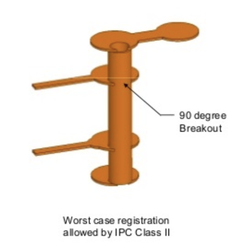
Image credit: ACDI
Instead of a 90-degree break-out; we would add the limit as “tangency”. Putting this into practical perspective, an 8-mil finished hole would have a capture pad of 18, 20 or 23 for classes 2, 2.5 and 3 respectively. The 8 mil callout with the 20 mil capture pad would give most fab shops a crack at achieving a no break-out requirement on the vias.
Bigger is Better
The larger diameter pad opens the process up to account for layer-to-layer misregistration in lamination as well as the positional and size tolerances of the drill process. There can be more than one way to achieve the desired outcome. The freedom grows with the layer count. Inner and outer layer line-width play a key role in setting the parameters the fabricator can dial in to make the PCB.
The other levers the shop can pull are mainly based around the dielectric materials available. What you imagined as a single core material wrapped in a few successive layers of prepreg material could turn out to use two cores joined by one layer of prepreg. How the layers are laid up matters, especially when controlled impedance lines are in play. Wake me up when they are not in play. The point I’m trying to make is that plating a hole is tricky and dependent on a number of factors, much of which, I just glossed over.
Finished Hole Size Equals Zero?
Right on the heels of the plating spec is the plating spec. The vendors want to be able to ship boards even when the hole winds up at the end of the process with no actual hole remaining to measure. Plated closed or plugged with a mask, smaller holes should have a negative tolerance equal to the nominal value. A range of sizes from 11 mils to zero by using unequal tolerances; 0.08” +0.03”/-0.08” for example.
Clip or Move the Silkscreen Away
Who hasn’t made some last minute part switch and processed the artwork with a glaring mistake on the reference designator layer? It’s almost automatic for me as I’m copper focused to a fault. Good thing the DFM tools keep getting better in terms of non-metal design rules. My rule of thumb is that I want my silkscreen lines to clear the soldermask openings by three mils. When it comes to flex circuits, way far away is the goal because I’m tired of hearing about it from those jobs. It may be the fab-houses I work with or it may be that flexes are hard to silkscreen.
Exposed Metal
Sending out data with the soldermask exposing a sliver of metal is usually harmless but generates a red flag because nobody wants to be responsible if there is a subsequent short circuit. I made one of those rows of numbers with a 1 on the top and 14 on the bottom with all of the layers between so you could sort of tell if the layers were not in the correct order. The copper flood on all layers was relieved and then I opened the mask for maximum visibility. My mask rectangles neatly overlapped the metal layers when they were supposed to contract. All I could do when I heard about it was to implement another quick DFM check before committing to turning pixels into printed circuit boards.
Stack-up
If you figure that you’ll be in a rush at the end, (surprise!) it will be beneficial to have the initial stack-up blessed by the vendor. Even if you’re not the one in touch with the actual vendor, say you’re working with an Original Design Manufacturer (ODM), it’s still a good policy to try to share that data to the point where they give you the line widths and material geometry that is exactly what they expect to build. Unless you were in a really tight loop with your supplier, I’d be reviewing the stack-up even when it comes to design reuse. How would you know that what was put to bed in the original docs was exactly what came out of the factory? Your technology needs to be in the moment. Arm yourself accordingly.
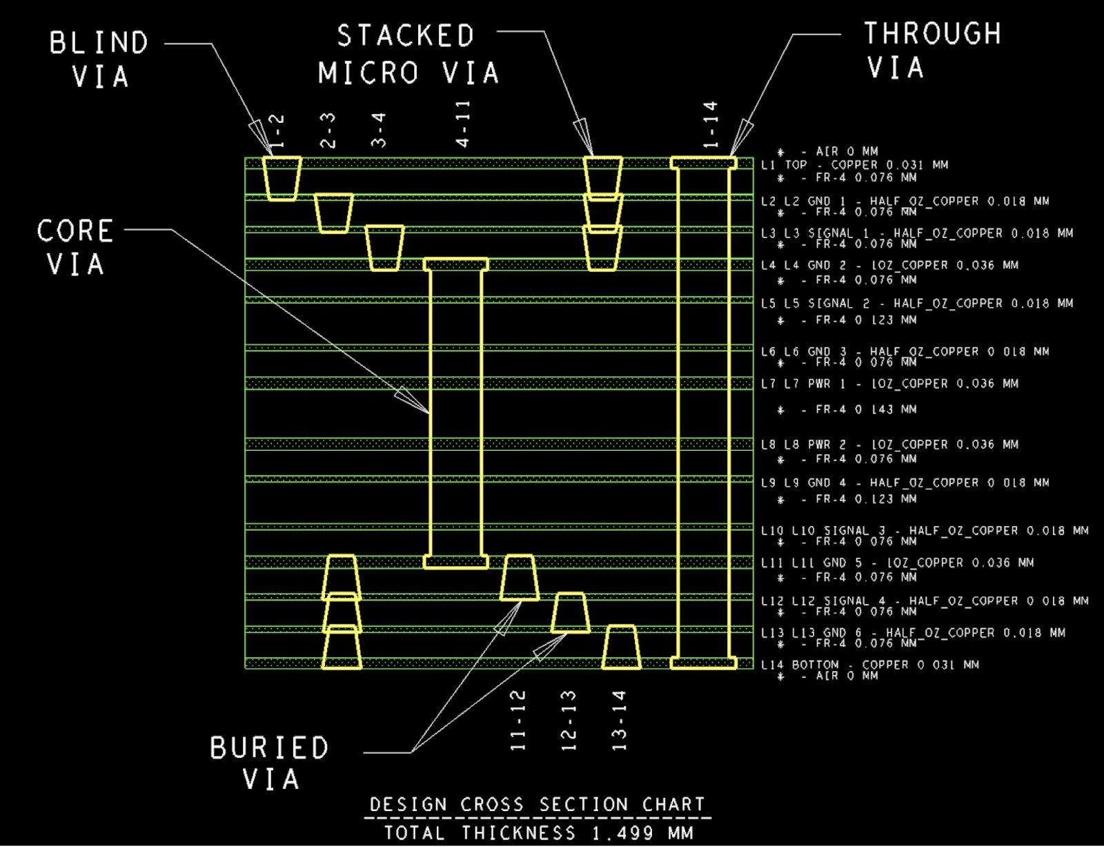
Image credit: Author - typically designated as a 3-N-3 stack-up; (through via optional)
Did I mention stack up? This will get you more often than not, especially with a flex circuit. Pave the road to success with an attachment to your fabricator. This gives them a heads up to get their hands on some of the material they will need to fill your order. They might even have a panel or two worth of material that they can set aside for you. This stuff has a shelf-life. That little fact could steer them towards suggesting the stack-up material and thus, the design criteria that you need to build into your design constraints to get everything right the first time. What you provide to them on tape-out day will limit what they can achieve, impedance wise. When you’re in a hurry, it’s worth slowing down a little bit to speed things up at the end.
One Last Thought
Find a way to retain those lessons learned. For me, a tape-out is a milestone that passes while I keep improving the design for next time. If three out of three vendors provided the same feedback on some aspect, you can bet the documents should take that into account. We can’t afford to sit still. Never stop learning. Never stop growing. Thanks for reading.