Printed Circuit Board Design For Assembly: How to DFA
Did I ever mention that I worked on an assembly line? Yup, way back when we used lead in our solder and freon to clean the flux off of the boards. It was hazardous to the environment and the assemblers. Things have improved for the environment but I’m not so sure I can say that about the workers. Through-hole components were a breeze to install and rework if necessary. We’ve come a long way towards shrinking the products and that comes with the cost of shrinking the components.
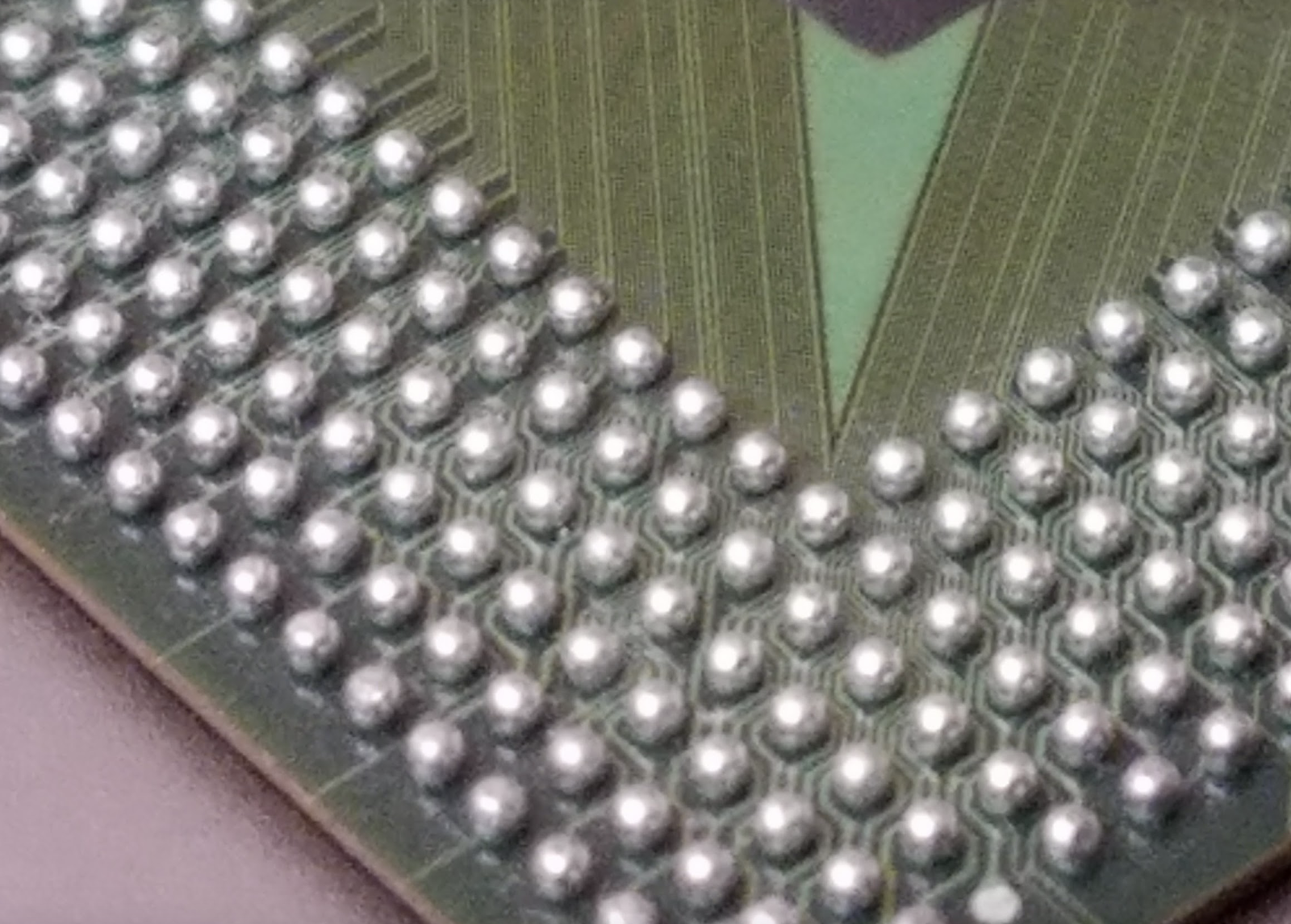
Image Credit: Author - FPGAs drive circuit density with flexible architecture.
Doing more with less has been a central theme ever since I moved from the assembly line to the CAD cave. Surface mount resistors and capacitors were just becoming a thing. DIP packages were slowly being replaced by SOIC equivalents. Up to that point, we measured the pin to pin pitch in fractions of an inch.
DFA Used to be Easy. Those Days Are Gone
A resistor was big enough to have four or five bands of color so that we could determine the value and tolerance at a glance. The leads were formed so that they could be inserted into holes that were a half of an inch apart. The popular 14 and 20-pin DIP (dual in-line package) used a tenth of an inch between pins down the sides with three tenths across the package. That’s huge!
Metrically, we’re talking 2.54 mm and 7.62 mm respectively. The first SMD components were half of that pitch but still, a 1.27 mm pitch device seems very coarse when we compare it to 0.5 mm of recent times. Not only that but the pins are not restricted to the two sides anymore. They go all of the way around in a quad-flat-pack arrangement.
Honey, I Shrank the Components!
That’s still not enough so we filled up the entire bottom of the component with little solder bumps instead of actual leads. We call that a Ball Grid Array, (BGA). Those devices have evolved from 1.27 mm pitch down to 1 mm then 0.8 mm followed by 0.65, mm, 0.5 mm, 0.4 mm and now 0.35 mm and even 0.3 mm in some cases. Electronic component assembly that had 0.1” to work with now got down to 0.016” or less. Murata has a new class of capacitors below the size of 01005. Get ready to work with values up to 0.1µF, 6.3vdc caps in 008004 (.25x.125mm) packages.
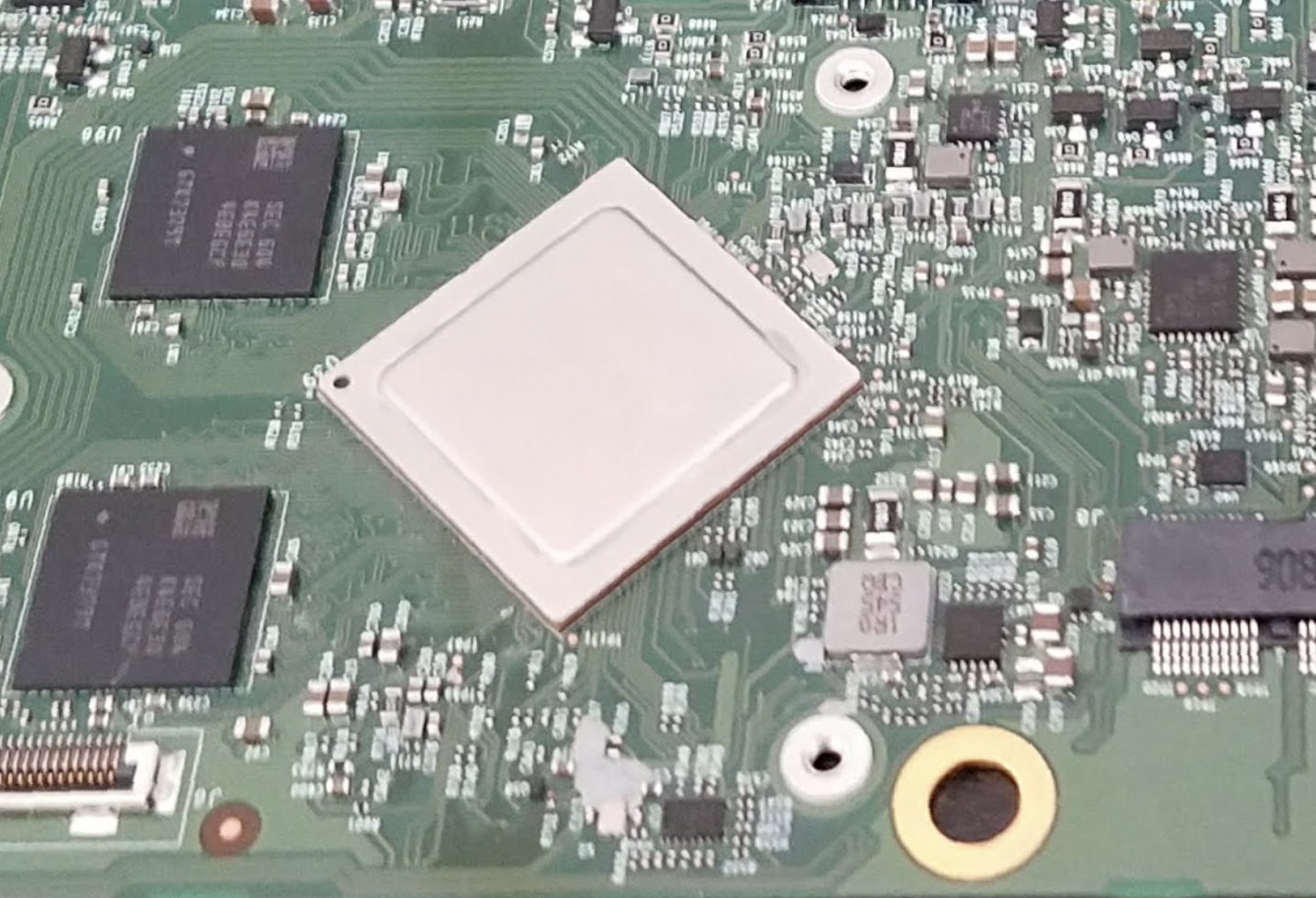
Image Credit: Author - Sometimes, placement requires a little creativity. Try not to be too creative.
All of this happened while we had to give up on SN63 solder. That is the magic formula of eutectic solder, 63% tin and 37% lead. The beauty of eutectic solder is that it has a nice low melting point and that it solidifies over a very narrow temperature range. Common lead-free solders have a higher melting point and are not so forgiving in the process window.
I said all of that to point out that PCB assembly is a lot harder than it used to be. The PCB materials have to withstand searing heat that can cause all kinds of problems. Any imbalance of copper in the board’s construction will have a greater tendency to cause warpage and twist as the board comes out of the IR oven. Imperfections in the finish coatings can result in blistering, measling, lifted pads, delamination or any number of solder defects.
Metal Migration in a Greener World
The metallurgy of RoHS compliant solder often features a good deal of tin with trace impurities of silver, antimony and other metals. In its pure form, tin has a nasty habit of spreading out and causing shorts. Not only in the solder joints where “tin whiskers” are common but on the traces themselves. Dendritic growth can form and cause shorts between adjacent traces.
Certain conditions of heat, humidity and higher voltage can give rise to the growth of conductive anodic filaments (CAF). This is where the dielectric materials break down and conductive salts can creep through the micro-cracks between the conductors. Again, this is all related to the greener board materials we are compelled to use to save our planet from toxic pollution.
The most important thing we can give the fabricator is a little extra space between conductors. Meanwhile, the most important thing we can give to the Marketing team is a super-small PCB. We designers have to walk a tightrope at the intersection of marketability, quality and reliability. Winning on all three counts is never easy.
Component Placement Tips for DFA
Placing passive components too near the edge can cause one pad’s solder to solidify before the other. The result can actually crack a ceramic capacitor or pull the wire of an inductor or wire-wound resistor away from the terminal. The metal parts can still be in contact but not bound to one another. If you must crowd the edge of the board or a slot within the board, try to place the parts horizontal to the edge rather than having one pin closer to the edge.
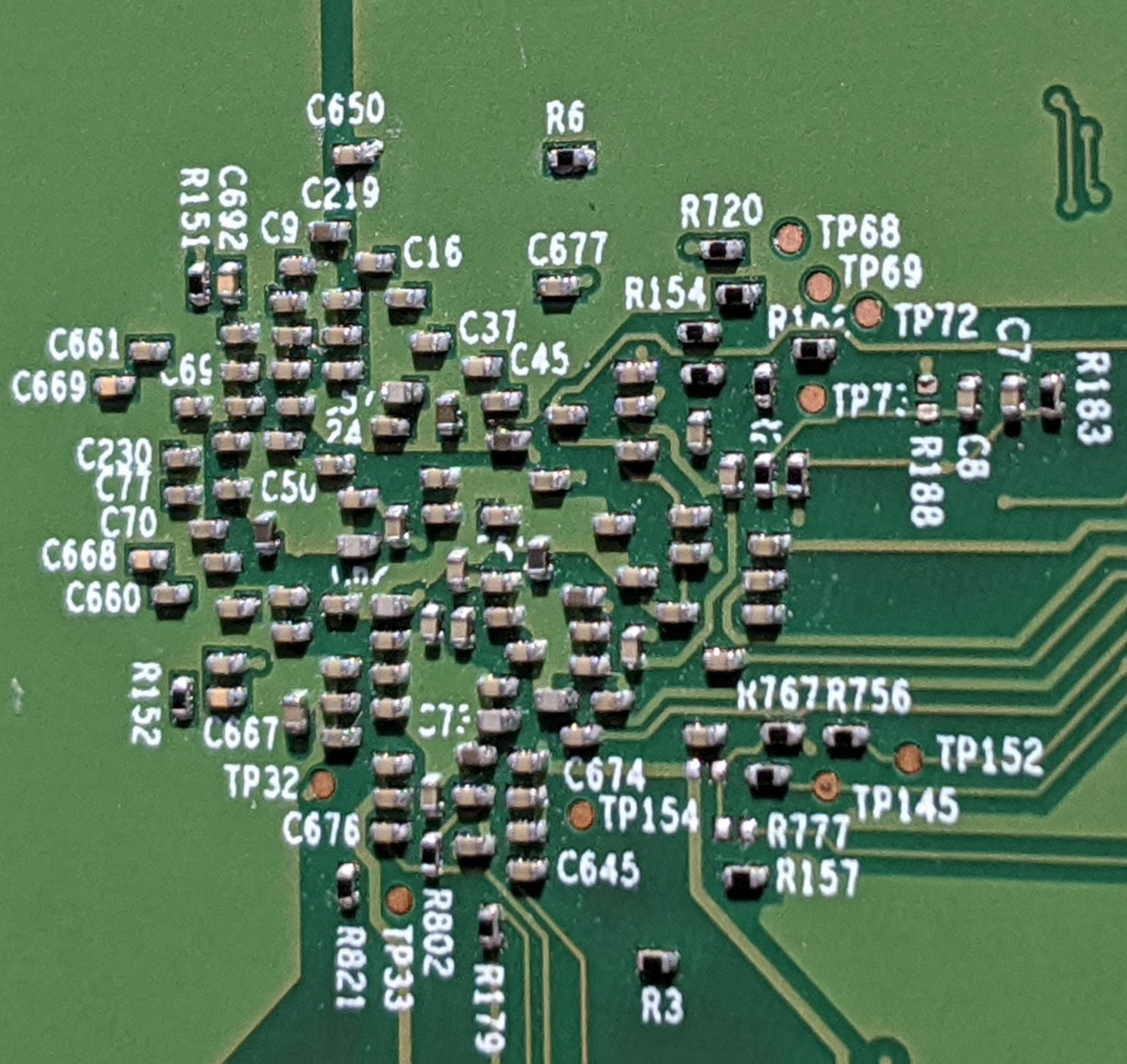
Image Credit: Author - If you can’t get all of the parts facing the same direction, favoring one orientation over the other helps.
If you’re working with BGA components, note that there is no direct access to all of the pins with a soldering iron. In order to remove and replace a BGA, a custom size nozzle fits over the component body and hot air is blown through the rework head to get all of the balls up to reflow temperature so that the component can be removed. That rework tool requires a certain amount of space to operate. If the area is occupied by components, then those components have to be removed first.
Raising Reliability While Reducing Real Estate
In high reliability, rough use applications, it is often necessary to underfill a BGA component. The BGA itself is a carrier for the silicon which can resemble a smaller version of the BGA with a grid of pins but on a smaller pitch. Those “flip chips” can be soldered directly to the board and will always require an underfill.
Wirebond style chips can also be installed on the board itself but you’ll want selective soft gold or an ENEPIG finish to accommodate the wire bonds. Either way, the whole chip gets encapsulated to protect it the same way the package would. In all of these cases, extra space is required around the part for the application of the underfill and/or encapsulant materials.
As always, it pays to consult with the vendor on the fabrication aspects. At the same time, that is to say early in the design phase, it’s important to have a dialog with the assembly house regarding their abilities with regard to component spacing. As a bare minimum, every component pad should have a solder mask around it with a dam of 100 microns or more. That geometry can guide placement of the smallest parts while larger, especially taller parts will want more space than that.
To Silk or Not to Silk - That is the Question
Of course, you know that we need good marking on the PCB to ensure that the correct components are placed with the right orientation. Given the shrinking real estate, there is a hierarchy of silkscreen elements. When you can’t fit everything, the first thing to go is the reference designators. It would be nice if there was some slack space to offset the reference designators from the high density regions as they do on paper maps of condo-complexes where all of the streets have long names and only two or three actual structures.
Next item for deletion is the component outlines. Some production boards leave it all off to save a few pennies. If you have nothing else, the pin-one marks are the thing to fight for. If you’re doing an ultra-dense placement, try to consider that little space around pin-one as a required marking zone. In a pinch, it can be done on the soldermask or even the metal layers.
The vendor has some of their own requirements like a date code and we want something to identify the part number and revision so we know what we’re dealing with. It helps to account for this minimal marking during the placement phase. While you’re at it, make sure you have fiducial marks and tooling holes. If they cannot possibly be on the board itself, they can be provisioned on the assembly sub-panel using the grab-rails or other break-off material. There are a lot of factors that can cost you money and time. Getting an early start to DFA will pay dividends at the end.