Vias: Types and Applications
Key Takeaways
-
The different types of PCB vias and their applications.
-
Some important details about vias that should be considered.
-
Setting up and using vias in PCB design CAD tools.
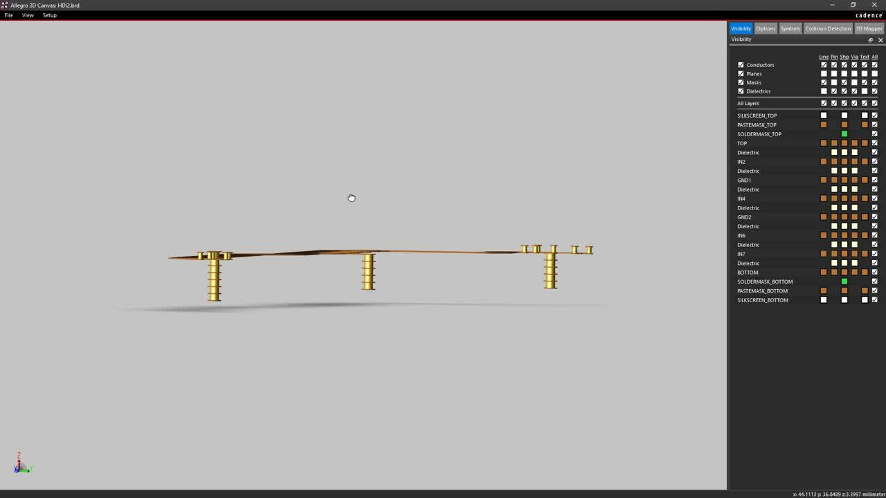
A 3D view of both through-hole and HDI vias within a design.
In our house, we have a laundry chute, and although they’ve steadily denied it over the years, I’m pretty sure my kids use that chute for more than just their dirty clothes. After all, why take the time to walk down the stairs when you can slide down the chute and quickly end up in the kitchen instead? As a parent, I certainly don’t condone this mode of travel, but as a PCB designer, I admire their ingenuity. Let’s face it, compared to the hallway and stairs, the laundry chute is--just as a via is in a printed circuit board--a very short path between the two levels of the house.
Using vias in a PCB design allows the designer to shorten the distance that a trace must be routed in order to complete its connection. Just as with the laundry chute, the via will drop the trace down onto another layer where there is a clear path, instead of wandering the long way around. The important thing is to understand what the different via types and applications are in order to use them effectively for the purposes of both manufacturing and signal integrity. Let’s take a look at the different vias that are available to PCB designers and how they should be used.
The Different Types of Vias and Their Applications
Vias are metallic lined holes connected to the metal circuitry of a PCB that conduct an electrical signal between the different layers of the board. Although vias can vary in their size, pad shapes, and hole diameters, there is only a handful of different via types or structures:
-
Thru-hole via: This is the type of via that is used most often in a circuit board. The holes are drilled all the way through the board with a mechanical drill bit and can get down to 6 mils in size.
-
Buried via: This via only connects internal layers of the board and is useful for PCBs with very dense routing.
-
Blind via: This via starts on either the top or bottom of the board but doesn’t go all the way through it.
-
Microvia: For hole sizes smaller than 6 mils, a laser-drilled microvia is used. These vias connect only two adjacent layers of the board and can be on the surface or buried within the board layer stackup. Microvias are extremely versatile and can be stacked together, or on top of a buried via, but have a higher fabrication cost associated with them.
-
Via-in-pad (VIP): These vias can either be standard thru-hole vias or microvias, but their position in a surface mount pad makes them unique. If a standard mechanical drill is used, the via will require extra fabrication steps to prevent solder on the pad from flowing down through the hole. Microvias on the other hand don’t have this problem, but they can be more difficult to fabricate due to the tighter trace and space tolerances in a high-density design.
Ultimately, which type of via to use depends on the technology of the printed circuit board, the circuitry needs, and the targeted cost of PCB fabrication. For instance, a microvia is very desirable to use because of its smaller size, but that doesn’t necessarily make it the best choice. A microvia has more steps involved in its fabrication and, therefore, is more expensive compared to a mechanically drilled thru-hole via. But if you are designing a high-density interconnect board, the microvia becomes the better choice. Here is a breakdown of the common uses of vias in PCB design:
-
Signal routing: Most circuit boards will use a thru-hole via for signal routing placed on a grid. Denser boards, however, may also use blind or buried vias, while very dense boards will need microvias.
-
Escape routing: Larger surface mount (SMT) components can usually have their escape, or fanout, routing done with thru-hole vias. In some cases, blind vias or microvias will be used, and on very dense packages such as high pin-count BGAs, a via-in-pad will be used.
-
Power routing: Since the vias used for power and ground nets will conduct more current, they are usually restricted to larger thru-hole vias, although blind vias may be used as well.
-
Stitching vias: These vias are used to provide multiple connections to a plane and are, therefore, thru-hole or blind vias. For example, a sensitive area of circuitry may be surrounded by a strip of metal with vias stitched in it to connect to a ground plane for EMI protection.
-
Thermal vias: In this case, a via is used to conduct heat from a component out through the internal plane layer that it is connected to. This usually requires a larger thru-hole or blind via and these vias are often in the pads of these devices as well.
Now that we’ve seen what vias are and how they are used, let’s drill a little deeper into some of the considerations for using vias that PCB designers should be aware of.
Be cautious of groups of vias that could block off the signal return path in a ground plane.
Important Considerations about Vias
Before a PCB layout designer can start dropping vias into their board design, there are a few more details about vias to be discussed. We’ve already talked briefly about the difference in the manufacturing costs between a thru-hole via and a microvia, which can be a real wake-up call if you aren’t prepared for it. Now, here are some other considerations to keep in mind as well.
Aspect Ratio
When using a mechanical drill to create a standard via, it is important to remember that the smallest acceptable drill size is based on how thick the circuit board is. Mechanical drills have a limit to how much material they can drill through before they become unreliable. This is measured by the relationship of board thickness to drill size, and PCB fabricators will usually require an aspect ratio of no more than 10:1 for their drill sizes. This means that for a circuit board that is 62 mils thick, the smallest mechanical drill size that you should use is 6 mils or 0.006 inches. If you need a hole smaller than that, you should look into using microvias which have an aspect ratio of 1:1.
Annular Ring
The size of the via pad is important. You need to ensure that a large enough annular ring remains after the via is drilled. A mechanical drill will wander a little while it is drilling, and without a sufficient annular ring, the via may be compromised by drill breakout.
Signal Integrity
Although a via is very short, it is still a measurable length of the conductor which could cause problems with tight signal integrity requirements. For instance, a thru-hole via that connects the top two layers in a ten layer board will have 8 layers of unnecessary metal in it that could create interference. It is important to find problems like these and remedy them with techniques such as back-drilling the via to remove the unused metal from the line before it acts as an antenna. Here is where the signal integrity analyzers of PCB design tools like Cadence Allegro can be very helpful to the designer in finding these problems before the board goes out for manufacturing.
Routing Density
In situations where dense areas of the board are being routed, the designer must take care that they don’t block up routing channels or ground plane return paths with vias. This can happen under dense parts like high pin-count BGAs where there are hundreds of vias in one small area. This is where the use of blind vias and microvias becomes essential in planning out the BGA escapes so that every pin gets routed but important routing channels and planes are not blocked off under the part.
With these considerations now in mind, it’s time to start instantiating vias in a design. Next, we will look at some features in PCB design systems that will make the job a lot easier.
The Padstack Editor inside of a PCB layout tool system.
Creating and Using Vias in Your PCB Design CAD Tools
For the best results when working with vias in a PCB design, you need a CAD system with both power and flexibility. Not only do you need the tools that can create the precise vias that you need, but you will also need some advanced features for using those vias as you route your board.
-
Via creation: The first step is to create the via, and as you can see in the picture above, having an advanced padstack editor, like what is available in Allegro PCB Designer, is really helpful. With it, you can specify not only the pad shapes and sizes for the different layers, but you also have control over drill sizes, tolerances, and offsets.
-
PCB libraries: Once the vias are completed, it helps to be able to park those vias in a library where you can use them again and again. This will save you a lot of time and frustration in future designs by not having to constantly reinvent the wheel.
-
Routing tools: The next step is using the vias while you route, and Allegro has this covered as well. Not only can you manually instantiate your vias while you route, but there are many automated features like fanout routers that you will find useful.
-
Advanced features: Allegro’s enhanced functionality will elevate your usage of vias to the next level. Take for instance, via structures; this unique feature will combine vias with traces, shapes, and keep-outs in order to create automated fanouts with high-speed properties.
-
Design rules: With the Constraint Manager in Allegro PCB Designer, you will have control over which vias are used for each individual net.
Allegro PCB Designer’s Constraint Manager displaying different nets and their via assignments.
There are many ways to create and use vias in PCB design, and we’ve only scratched the surface here. For more information on routing your printed circuit board, take a look at this E-book on routing.
If you’re looking to learn more about how Cadence has the solution for you, talk to us and our team of experts.