PCB Via Placement in High-Speed Designs
Key Takeaways
-
Setting up your design for the most optimum via placement.
-
Some ideas on via placement for escape routing.
-
Via placement that will help you to control signal integrity in your high-speed design.
3D view of vias in a high-speed design
When designing a printed circuit board, there is a lot of placing that needs to be done. To start with, all of the schematic symbols will need to be placed. Then they will probably get moved and re-placed many more times before the schematic is completed. Once you get into the layout, each component will be placed. And as with the schematic, these parts will also get moved a lot in order to optimize the placement for the best circuit performance and manufacturability.
There’s another part of the layout that needs to be placed though, and those are all of the vias in the design. If you’ve never thought of adding vias as “placing” them, you’re not alone. Vias are usually considered to be part of the trace routing process. Route horizontally until you run into an obstacle, then via down to the next layer and run vertically. But that kind of thinking needs to be challenged when it comes to via placement in high-speed designs, where vias can have a huge impact on how the board performs.
Setting Up for Via Placement in High-Speed Designs
One of the best things that you can do to help yourself place vias on a high-speed design is to get yourself organized first before you jump into the layout. This means getting your design setup for all the basics that you would do for any type of PCB layout. You will want to make sure that your schematic is clean and completed as much as possible, and that you understand the layer stackup that you will be using in your layout. You should also make sure that your PCB footprints and other library parts are current and ready to go, and set up your grids and other design parameters.
Another part of your design setup will be the preparation of the vias that will be used in the layout. These are often available in PCB part libraries, or you can create them in the CAD tools yourself. The vias that you set up should be associated with the different nets and design constraints of your layout so that the correct via is used in the appropriate locations. High-speed designs will require a mixture of different sizes and types of vias:
-
Thru-hole: This is the standard via type that is used on virtually all PCB layouts, and is drilled through the top to bottom layers, connecting all the layers throughout the pcb. You will need larger thru-hole vias for power and ground connections, and smaller vias for regular signal routing. In some cases you may need a mixture of different sized vias depending on the current loads of the nets that you are routing.
-
Blind and buried: A blind via starts on an external layer, either top or bottom and terminates within an inner layer. A buried via on the other hand starts and stops on inner layers. These vias cost more to fabricate but can be an important part of routing dense designs.
-
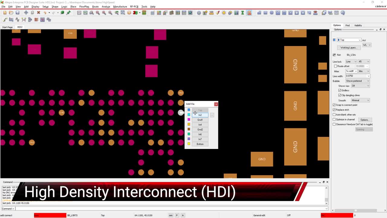
Microvia: Instead of being created with a regular drill, a microvia is laser drilled allowing it to be much smaller. It is very important in high-density designs, and you can see an example of how to create a microvia using the Padstack Editor in the Cadence Allegro PCB Design system below. To read more about preparing a design for successful routing, take a look at this linked information.
Using the Padstack Editor to create or edit Microvias in Allegro PCB Designer
Vias Used for Fanout Routing
Once you start into the design, you obviously have to place your components before you can route them, but you still need to keep your eventual routing and via patterns in mind. You will want to start with your main components and group the circuit paths together, and then add the smaller parts around them. When placing your decoupling capacitors, remember that a via that connects an IC power pin to a capacitor on the opposite side of the board has a lot more inductance than if the parts were both on the same side.
Placing vias to connect decoupling capacitors to ICs is only part of the escape routing that you will be doing. Most all of the surface mount parts including ball grid arrays (BGAs) will need to have vias added to them for access to inner layer routing channels. Here is where using a design grid for your vias can be a big help:
- Using wide grids for via spacing will allow for greater routing channels between them.
- Vias should be placed strategically to allow for routing in different directions as well as turning large busses of traces.
- Vias on a grid that are aligned with placed components will offer more routing channels than vias placed at random.
- In some instances, it is better to route away from the part and then drop the vias to avoid blocking the routing channels.
Your PCB design tools will give you a lot of options for setting up design grids that can help with your via placement. You can see some of the design grids that can be set up in Cadence Allegro PCB Designer in the picture below.
Placing vias can be simplified by setting up the appropriate grids
When routing out of fine pitch BGAs, you may have to use smaller vias, vias in pads, or microvias to get all of the escape routing in. Regular drilled vias in BGA pads are very helpful for this but will require an extra fabrication step to prevent solder from wicking away from the part through the hole. Microvias in the BGA pads are also very helpful but can be more difficult for fabricators due to the narrow trace and space tolerances in a high-density design. Remember that when you escape route out of a high-pin count part like a BGA, it is important that your via patterns leave room for inner layer routing channels.
Vias and Signal Integrity
Once you’ve finished with the escape routing it is time to start connecting the nets together in etch, but you still need to be careful how you route and place vias in a high-speed design. We all know that a trace on a PCB has inductance, but so does a via. Although the length in a via is very small compared to the trace, it can still make a difference in the signal integrity of a very high-frequency line. So it is best to minimize the use of vias as much as possible. This will help you to avoid any additional inductance, length, or other signal integrity problems that the extra vias may cause high-speed or RF designs. For more information on some best practices to use when designing with RF signals, use this link.
Another concern with via placement in high-speed designs is routing differential pairs. You will want to avoid using vias as much as possible, but it is usually difficult to do that. When you do use vias in differential pairs, put vias in both traces to make them equal. Also, when routing a differential pair around a via, make sure that you don’t split the traces around both sides of the via. Both lines need to be kept together.
When placing your vias for either escape routing or bus routing, be careful to not create a continuous void in the ground plane. The overlap of the antipads in a plane could create a slot as shown in the picture below. This void can block the clear signal return paths through the plane causing the return signals to wander around trying to find their way back. Blocking return paths like this can result in increased electromagnetic interference (EMI) and signal integrity problems for the board. For more useful information on designing a good power delivery network (PDN), go to this link.
A line of vias can create a void in a plane, and block the return path of high speed signals
Another concern about vias in a high-speed design is via stubs. When using a thru-hole via that connects layer one to layer two, the via will still continue on through to the other side of the board. This excess amount is a stub on the line which could cause unwanted signal reflections. These stubs can be eliminated with a fabrication process called backdrilling, or the use of blind and buried vias can restrict the via stack to just the layers that it is connecting.
Another via placement technique in high-speed designs that is helpful is to place “stitching” vias around specific objects on the board, or around the board outline as a whole. The Faraday cage effect created by the stitching vias helps to suppress potential EMI problems in the board by preventing any of the board objects acting as antennas. Also by connecting all of the ground planes of the board together with stitching vias, it helps those planes to remain at the same ground potential which helps promote better signal integrity. To learn more about how to achieve high-speed design success, take a look at this E-book.
Using Your PCB Design CAD Tools to Work with Vias
As you can see, there’s a lot more to a via then merely connecting a trace up in a high-speed design. How you do or don’t work with vias can have a huge impact on how your design will ultimately work. Thankfully your CAD tools can offer a lot of help with this by giving you ways to create, modify, and manage your vias. You can also work with grids, design rules, and constraints to govern which via is used for specific nets, layers, or areas of the board.
Make no mistake, this level of control requires a PCB design system that has cutting-edge features and capabilities to support the different types of via management needed for high-speed designs. Allegro PCB Designer has been created for advanced PCB layout work like this and is the design system that you need to support your high-speed printed circuit board design.
If you’re looking to learn more about how Cadence has the solution for you, talk to us and our team of experts.