Ground Connectivity and High-Speed Signals in Multi-board Design
I recently got a dehydrator for my kitchen. It’s this massive, hulking box that is going to yield so many yummy things like chips, jalapeño powder, and fresh-foraged mushrooms. Of course, I wondered how many boards were inside if I cracked it open—if one board was controlling the whole process or if there were a few keeping things together and tracking separate things like heat regulation and the requisite sensors.
From TVs to laptops, many of our favorite consumer electronics are really multi-board systems. Open up your laptop or desktop, and you’ll find a rich multi-board system with cables and onboard connectors linking your motherboard and peripherals in your system. With computer peripherals running faster, proper grounding and maintaining clean high speed signals in multi-board designs is critical for keeping bit error ratio (BER) values low and passing EMC testing.
High Speed Design Within Each Board
Individual boards within a multi-board system should always be designed to ensure signal integrity in a high speed system. High speed signals within the board should be routed to prevent crosstalk and ringing due to transmission line effects, as well as have proper, uninterrupted return paths to maintain signal integrity. Grounding is also an important issue in an individual board, but it becomes even more important when high speed signals are sent between boards as part of a multi-board system.
The important point in high speed design that many novice designers miss is this: the data transfer rate does not determine whether a board is classified as high speed. Instead, switching speed between the ON and OFF states is what classifies a board as high speed.
Modern digital ICs are being built successively smaller, which reduces their gate capacitance and switching time. Even if you are working with a communication protocol with a lower data rate such as an serial peripheral interface (SPI) bus, newer digital ICs will switch fast enough for your device to be classified as a high speed device.
Keeping this in mind, you’ll need to check your interconnect lengths against the switching time in your circuits when designing your board. If 25% of the signal rise time (10% to 90%) is less than the propagation delay along a trace, then the trace will act as a transmission line, and you will need to impedance match the trace to the source and load, add termination at the source or load, or use impedance controlled design to ensure the trace impedance matches the source and load. This will prevent reflections that lead to ringing in digital signals.
When routing a signal net with parallel data, you’ll need to make sure that your signals within the net are synchronized to prevent timing skew. Timing skew should be compensated within an individual board, as well as between boards, lest unsynchronized signals lead to high BER values. This requires length matching traces within a signal net, including length matching between differential pairs. Be careful with differential pairs and try to enforce symmetry in your routing and length matching scheme where possible.
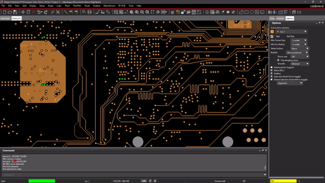
Ensuring proper trace routing is one of my favorite tasks in design
Grounding and High Speed Signals in Multi-board Design
When routing high speed signals between boards in a multi-board system, you will need to design your connection so that your signals have a reliable return path back to the ground. If you neglect this, then your return signals will be forced to take the long route through the ground connection on the destination board, back through the power supply or chassis, and into the source board. In essence, you’ve just created a giant loop antenna, and your system will likely not pass EMC checks.
The easy way to do this is to use differential signaling when sending signals between two boards. However, this requires components on each end of the board that support differential signaling, which is not always possible. This does not accommodate every communication protocol (I2C, for example).
Where differential signaling is not possible, you will need to take advantage of the ground plane on the source and destination boards to provide a return path for signals routed between boards. Consider, for example, two boards connected to a power supply. The source board provides some processing with an FPGA or other components, and the destination board contains some peripheral components that need to receive some data.
In order to provide a short return path for signals routed between these boards, you will need to include a grounded connection that runs across your connection. You can connect one pin on the connector in the source board to the source board’s ground plane. You will then need to do the same with the connector on the destination board.
In essence, you now have a grounding connection in your connecting cable that is referenced to the same plane as your signals. This choice of reference is extremely important: you must reference this grounding connection to the same reference plane as your signals, otherwise you risk creating ground loops. If you have pins to spare, it is best to place multiple grounds in the connection between boards, preferably between neighboring signals, as this will reduce ground bounce during high speed switching.
Your computer peripherals will use multiple grounded signals on your board-to-board interface
Standard protocols for parallel data are actually designed with this grounding scheme in mind. If you look at the specifications for standard protocols, such as DDR4 or PCIe, you’ll find that the pin layout for these multi-board interfaces is specifically engineered with multiple grounded lines on the interface in order to provide multiple return paths for signals in the connection.
Using the right PCB layout and design software with a full suite of design tools makes it easy to include the important design features discussed here in a multi-board system. The design features in the Allegro PCB Designer suite allow you to implement important high speed design rules for single board and multi-board systems.
If you’d like to learn more about Cadence and get the best design tools for your next multi-board system, contact an expert today.