High Current DC Voltage Management in Power Systems with PSpice
What You Can Take Away
-
DC power distribution is all about tracking voltage drops throughout the system.
-
At high current, a significant voltage drop across a resistive element will convert power into heat, which will cause temperatures to increase.
-
If you can identify hot components before you create your PCB layout, you can determine whether you need fans, heat sinks, or more aggressive cooling measures in your board.
Do you know the right interconnect spacing and density you should use?
Every electrical engineer starts their electronics education by learning about DC power, Ohm’s law, and power distribution throughout a circuit. When you consider the simplified way in which real components are represented in circuit diagrams, DC voltage and current seem simple compared to AC power systems. In reality, DC power systems can get very complex, very quickly, and designers need to consider electrical and thermal safety in their systems.
Every digital and analog system will need an onboard power source, but boards for power electronics systems can be their own beasts. If you’re designing a DC power system, or you need a system for AC-DC conversion, you’ll need to consider the safety and temperature of your system, especially if it runs at high current. The term “high current” may seem a bit arbitrary, but the current in a system will determine the safety and temperature rise in different components as it determines the amount of DC power dissipated as heat.
High current DC voltage management in PCBs starts in your schematic. The goal is to examine how voltage is dropped across different components in the system and how much power is dissipated at high current. Components like resistors, transformers, switching FETs, and other driver or control ICs in high voltage/high current systems can reach high temperatures or expose a user to shock at the output. Thankfully, there are SPICE simulation tools that you can use to examine these aspects of DC power system design and determine the right layout choices.
DC Regulator Stages
Power systems themselves may need multiple regulator stages. The goal is to take an unregulated, possibly noisy DC source and convert it to a stable DC output with fixed voltage/current. When it comes to high-voltage power circuits, at high DC, there are very few ICs on the market that integrate all the required components for DC power conversion, so you’ll have to use separate discrete components on the input regulator stages. This is one reason these systems are quite large; discrete components need to be laid out on a PCB in order to make room for fans or heat sinks on the board.
In your schematic, you need to build out the regulator circuitry from discrete components and simulate the voltage/current reaching the output. The power provided by each regulator stage can be calculated using transient analysis in PSpice. By comparing the output power to the input power in each stage, you can determine the efficiency of the circuit. A well-designed switching regulator should have well above 95% efficiency. You can read more about designing and simulating various switching regulator topologies in a related article.

Schematic for a high-current DC buck converter
Here’s what you can simulate in your DC regulator stages with the simulation tools in PSpice:
-
Output voltage, current, and power. To do this, simply place an ideal load component (RL in the above image) and run a transient analysis. This will show you how the output voltage, power, and current rise to reach the steady state. Simply place probes across the output, or add waveforms. See the graph below for an example voltage waveform for the inductor in the above circuit.
-
Power dissipation in resistive components. Your goal here is to check that power dissipation in resistive components does not exceed absolute maximum power ratings. The power dissipation in each component will then determine its temperature rise. You can simulate the temperature in each component directly by including the components temperature coefficients as part parameters in your PSpice schematic.
-
Input DC voltage sweep. With a DC voltage sweep, you can see how the output from your system will change, and you can identify the maximum input voltage. This should be combined with the previous point as increasing the input voltage will increase the power dropped across different components. With switching MOSFETs, the output will saturate if the input voltage exceeds the linear range in the transistor’s load line.
A transient analysis allows you to see ripple on the output, the stable voltage level, and a comparison of the voltage ripple with the voltage/current in other components. An example that compares the output voltage with the inductor current in the above regulator stage is shown below. The image below also shows results for low input voltage. As you sweep the input voltage, you can generate multiple graphs and determine when the voltage level stops increasing (i.e., when the MOSFET in the regulator saturates).

Output voltage level and inductor current in a DC voltage regulator.
An important point to consider in the above circuit, and in your DC-DC converter design, is parasitics in the capacitor. Series inductance and resistance in the capacitor leads cause all capacitors to exhibit self-resonance, meaning the capacitor functions like a series RLC circuit. You can determine the self-resonance frequency for the capacitor using the frequency sweep simulation in PSpice. The capacitor self-resonance frequency should be larger than the knee frequency for the PWM signal to ensure low ripple on the output voltage.
Once you’ve determined the voltage and current in the DC-DC stages, you need to consider how your circuit
Isolation and PFC Circuits for High Current AC-DC Conversion
If you’re building a high-current DC power system that converts from an AC input, then you need a rectifier on the input. In order to maximize efficiency in the output from your switching regulator stages, you may need to use a power factor correction (PFC) circuit to ensure downstream switching regulators draw stable current. Switching regulators draw current in short bursts, so the current at the input power stage will not resemble a clean sine wave. Instead, it will appear as small bursts of current flowing through to the downstream regulator stages.
The point of a PFC circuit is to ensure the current reaching the downstream switching regulator resembles a sine wave. A PFC circuit uses an inductor on the output from the rectifier to dampen any current draw by the switching regulator. As the current burst flows through the output of the PFC stage, the inductor generates a back EMF, which slows the current rise reaching the input of the regulator stage. A typical topology is shown below:

PFC topology for AC-DC conversion at high current.
A PWM signal is used to switch a MOSFET (see S above), which causes the capacitor to charge and discharge. The output level and waveform from the PFC circuit will depend on the PWM duty cycle. The input inductor slows the rise and fall in the input current reaching the capacitor, which causes the current reaching the regulator input to resemble a sine wave with some ripple.
Just like the various regulator stages in your DC-DC conversion stages, you should perform a transient analysis on the output to check that your current waveform resembles a sine wave with ripple, and you should compare the input power with the output power to calculate efficiency. Resistive components should also be simulated for power dissipation, and you should check that power ratings and temperatures do not exceed maximum values.
The remaining aspect to consider in your high-current DC power system is isolation for AC mains. High power AC mains are normally fed through a transformer and rectifier before the PFC stage to step down the voltage. Using a flyback converter on the input DC regulator offers several benefits. First, the primary and secondary sides of the first DC regulator stage are electrically isolated. This reduces coupling of transients from the primary side, eliminates ground loops in downstream converter stages, and allows the output polarity to be controlled by choosing the winding direction on the transformer. A transient simulation in PSpice will show you how transients on the primary side propagate to the 1st-stage regulator output, which allows you to evaluate the safety of your system.
Planning Your PCB Layout
The results you receive from SPICE simulations are crucial for planning power distribution in your DC system. Your layout creates another layer of resistance to DC currents in the form of power/ground planes, vias, power rails, and real components. There are other aspects of your PCB layout that also need to be considered to prevent excessive temperature rise in your traces and components. These aspects of DC and AC PCB layout for high-voltage and high-current systems are specified in IPC standards as well as UL and IEC standards for consumer and commercial products.
For IPC compliance, there are two points to consider when starting a layout: current density in traces and spacing between conductors as a function of the potential difference between them. Trace widths in PCBs for DC and AC power systems can be sized based on the allowed temperature rise in the trace. This can then be determined from the IPC-2152 nomograph; the goal is to determine the appropriate copper weight to use in a PCB.
Spacing between conductors held at different potential is specified with the goal of preventing electrostatic discharge during operation. These rules for clearance (line-of-sight spacing) and creepage (spacing across a board surface) are specified in the IPC-2221 standard. There are some simple formulas that can be used to determine the minimum clearance and creepage distances in your high-voltage DC power system as a function of voltage.
Your PCB laminate needs to be plated with the right copper weight to prevent excessive temperature rise in your high DC current power system.
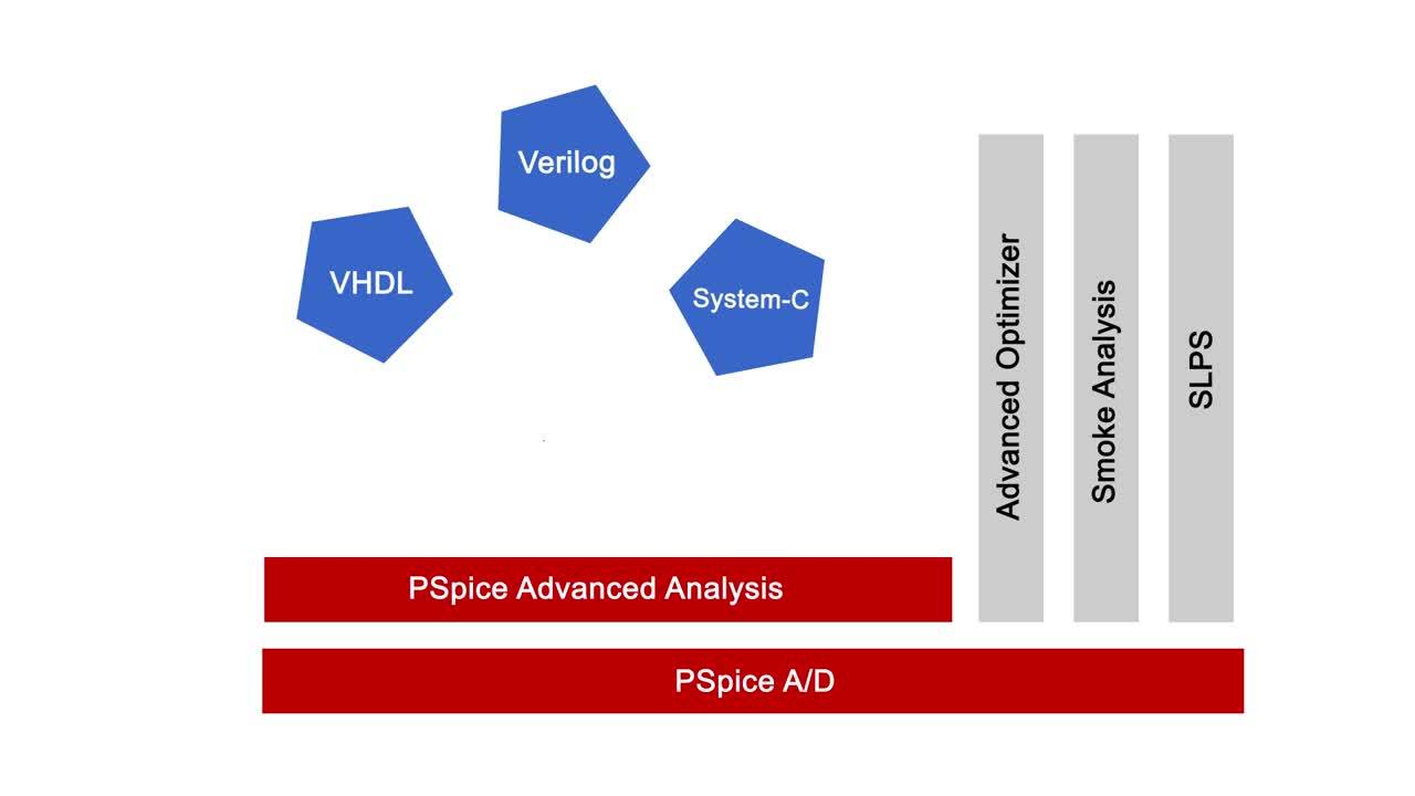
Once you’ve determined the right copper weight, trace width, conductor spacing, and heat management strategy for your board, the design tools in Allegro can help you create the perfect PCB layout. A powerful finite element multiphysics simulator is also available to examine how airflow and heat move throughout your system to help keep it cool. Finally, a PDN analyzer is useful for identifying specific hot spots in conductors as these cannot be identified from schematics. The design tools from Cadence provide everything you need to create PCB layouts for power systems as well as perform SPICE simulations.
If you’d like to read more about managing your power delivery network or working through the necessities of a power system, consider perusing our available ebook on PDNs.
If you’re looking to learn more about how Cadence has the solution for you, talk to us and our team of experts.