Why EMI Compliance Fails Despite Rule-Driven PCB Design
You ran the design rule check (DRC) on the PCB. It had zero violations. The board went out for fabrication, came back and completed testing just fine.
Then it got sent out for an EMI test and everyone crossed their fingers. Your colleagues come back with the lab results, and the radiated emissions plot has a peak that’s 4 dB over the Class B limit at 240 MHz. Nothing changed about the rules or your process. So, what happened?
Design rules enforce PCB shapes and geometry, letting you know if they’re allowed. But they do not tell you what the electromagnetic fields are going to do once power and signals are flowing across that PCB geometry. EMI compliance is a field problem. Rules are a geometry problem. The two are related, but they are not the same thing.
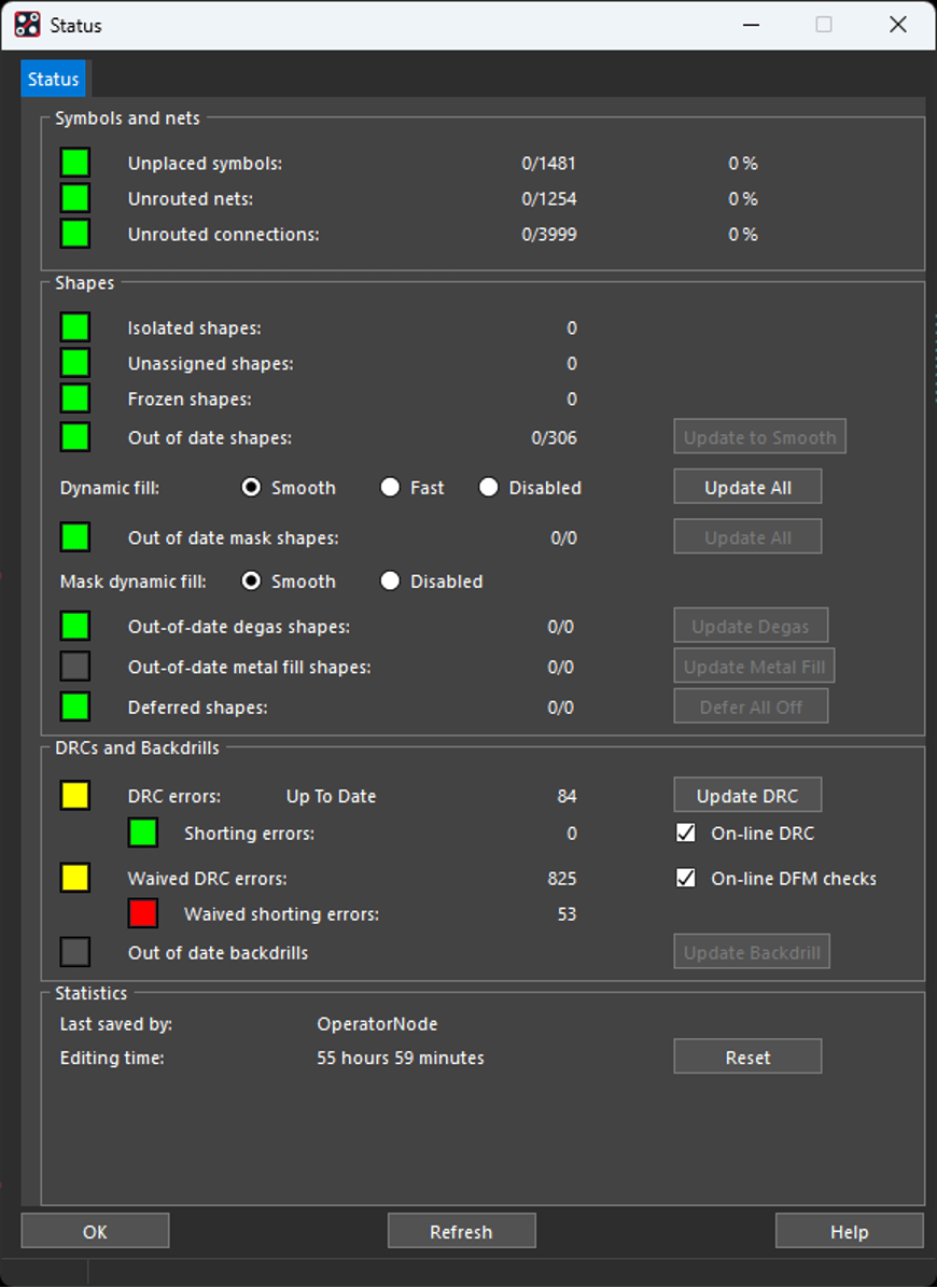
Figure 1. Allegro X PCB Layout DRC report panel showing zero violations.
What Design Rules Actually Check
A modern constraint system such as the one in Allegro X PCB Layout enforces things like trace width, clearance between objects, length matching across a bus, differential pair gap, via count on a net, and minimum drill spacing. These checks keep the fabricator happy and stop your board from shorting out on layer 3 before it ever ships.
What the rules cannot do is predict how the electromagnetic field moves through the copper. Whether a structure radiates, couples, or rings depends on edge rate, dielectric stack, plane behavior, and the frequency content of the signal. None of that is in a constraint.
A 5-mil trace clearance does not tell you the loop area between a signal and its return current. A length-matching tolerance does not tell you whether your return path crosses a plane split. A spacing rule does not tell you the cumulative coupling from six aggressors switching at once . The constraints answer one question, "is the geometry legal?" EMC asks a different question, "what is the field doing?"
Four Mechanisms That Slip Past a Clean DRC
Four electromagnetic mechanisms repeatedly appear in boards that pass every design rule yet still fail EMC compliance testing.
1. Return path discontinuity that grows loop area. At high frequency, r eturn current concentrates directly beneath the signal trace because at high frequency the path of lowest impedance runs directly under the trace, minimizing loop inductance. At DC this concentration effect is absent and the current spreads broadly across the plane . When the reference plane underneath that trace has a void, a split, or a layer change without a stitching via nearby, the waves must detour to find the same zero-volt reference conductor (typically called ‘ground’). That detour adds loop area and it radiates. The bigger the loop, the lower the frequency at which the structure becomes an efficient antenna (producing peaks at unwanted frequencies, essentially). So even if your trace still meets every line width and spacing rule, and your DRC report is flawless, that EMC chamber will still see spikes.
2. Common-mode conversion from imbalance. Differential pairs are supposed to radiate very little because the two opposing waves and fields cancel each other when received in the far field. That cancellation depends on the two signals staying balanced (equal amplitude, opposite polarity, same arrival time). When one half of the pair sees a different reference, a longer route, or a different via stub than the other half, some of that differential energy converts to common-mode energy. Common-mode current travels along the outer surface of attached cables, which act as the radiating antenna. Unlike differential-mode energy, common-mode has no cancellation mechanism, so even small imbalances produce emissions that escape the board efficiently. Sure, your pair will still pass intra-pair skew constraints, but the mode conversion from mismatched waves shows up in the chamber, not in the DRC.
3. Plane resonance and shared impedance coupling. A pair of power and ground planes is a parallel-plate capacitor, but it is also a resonant cavity . At certain frequencies set by the plane dimensions and the dielectric, the cavity rings. Switching currents from one part of the board pump energy into the cavity, and that energy couples into every other circuit referenced to the same planes. None of this depends on whether a constraint was met. It depends on plane shape, decoupling placement, and locations.
4. Edge rate is a variable that affects all three mechanisms. A signal with a 1 ns rise time has significant harmonic content above 300 MHz. Slowing that edge to 3 ns where signal integrity still allows it reduces the frequency content driving return path loops, mode conversion, and plane resonance simultaneously. Constraint systems do not enforce edge rate. That decision happens in component selection and termination strategy, which means it has to be made before routing begins.
How You Find These in the PCB Layout, Not the Chamber
Sigrity X Aurora reads the Allegro X PCB Layout database directly, so the analysis reflects the actual copper geometry without requiring a separate model.
For return path problems, the Return Path Workflow in Sigrity X Aurora flags signals whose reference planes are interrupted. Results show up as color-coded overlays on the canvas, and you can jump from the violation table straight to the location in the layout.
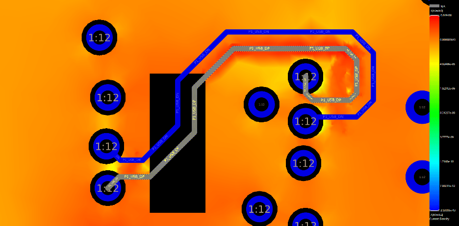
Figure 2. Sigrity X Aurora Return Path Workflow color-coded vision on the canvas, showing an intentional discontinuity and the return current disappearing around the void
For coupling between aggressors and victims, the Coupling Analysis Workflow highlights areas where energy from an aggressor net is most likely to couple into nearby victim structures. The results are displayed directly on the layout canvas, making it easier to identify potential EMI and crosstalk risks before detailed simulation.
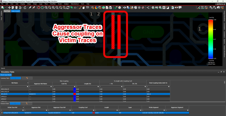
Figure 3. Sigrity X Aurora Coupling Analysis canvas vision with the coupling color gradient visible. Worst Case view mode highlights victim segment (in red)
For PDN problems that drive EMI, the PDN analysis workflow reports target impedance versus frequency. It also identifies decoupling capacitor placement issues that drive loop inductance up.
The Real Tradeoff
A board respin caused by failing compliance is two to four weeks for fabrication and assembly plus engineering time to diagnose and re-test. The analysis that would have caught the failure beforehand can be run during routing, before the design is committed to fabrication .
Design rules keep your board buildable. Electrical analysis keeps your board passable. Running both concurrently, rather than treating analysis as a post-routing step, is where most teams recover time lost to late-stage compliance failures .