How Does Energy Flow in a PCB? Understanding SI and PI
A common assumption in printed circuit board design is that electrical current flows in closed loops from source to load and back to the source. This model remains essential for circuit analysis, but it does not fully explain many of the challenges encountered in modern high-speed systems, including crosstalk, reflection, power distribution noise and voltage ripple.
To understand why these effects occur, it helps to look at how energy actually flows through a PCB. While electromagnetic fields govern PCB behavior at all frequencies, their effects become increasingly important in high-speed systems. Signal integrity (SI) and power integrity (PI) are strongly influenced by how these fields interact with the board’s conductors, dielectric materials, and reference structures such as ground planes, power planes, and other conductive surfaces that provide return paths for current.
Why the Closed-Loop Model Becomes Limited at High Speed
Circuit theory models current flowing through closed conductor paths, and this remains a valid and essential abstraction for analysis. Kirchhoff’s laws continue to hold under all operating conditions. However, at high frequencies and fast edge rates, this model does not explicitly describe spatial energy distribution in a PCB.
At high speeds, electrical energy transfer is better understood through electromagnetic fields that exist in the space surrounding conductors, with most stored energy residing in the dielectric between them. The conductors carry current and establish the boundary conditions that shape electromagnetic fields rather than serving as the primary medium for energy transfer.
This distinction becomes important when analyzing high-speed effects such as crosstalk, reflection, and power distribution noise.
How Energy Propagates Through a PCB
When a driver switches state, it creates a time-varying electromagnetic field. That change propagates through the surrounding dielectric, guided by the geometry of the conductors and reference structures.
In a PCB stackup, energy transfer occurs through coupled electric and magnetic fields shaped by layer geometry and material properties.
Conductors support this behavior by providing the boundary conditions that guide the fields and associated currents. However, current alone does not fully describe energy flow in the system. Electromagnetic fields carry the dominant energy transfer through the dielectric between conductors.
This field-based behavior explains why transmission line effects naturally appear in PCBs. The geometry of the conductors and reference structures determines how these fields are distributed, establishing the characteristic impedance of the interconnect and influencing how energy propagates through the board.
Return Paths as Field Structures
The concept of a “return path” is often described as current flowing back through a ground connection. While this is a useful circuit-level interpretation, it is more accurate at high frequencies to view return currents as part of the electromagnetic field configuration around the signal conductors.
The distribution of these currents depends on frequency, geometry, and the available reference structures. When geometry is continuous and well controlled, the fields remain predictable. When discontinuities appear, the field distribution changes based on the new boundary conditions created by the geometry. This can lead to unintended coupling , increased loop inductance, reflections, common-mode current generation, or unwanted radiation.
The Relationship Between Signal Integrity and Power Integrity 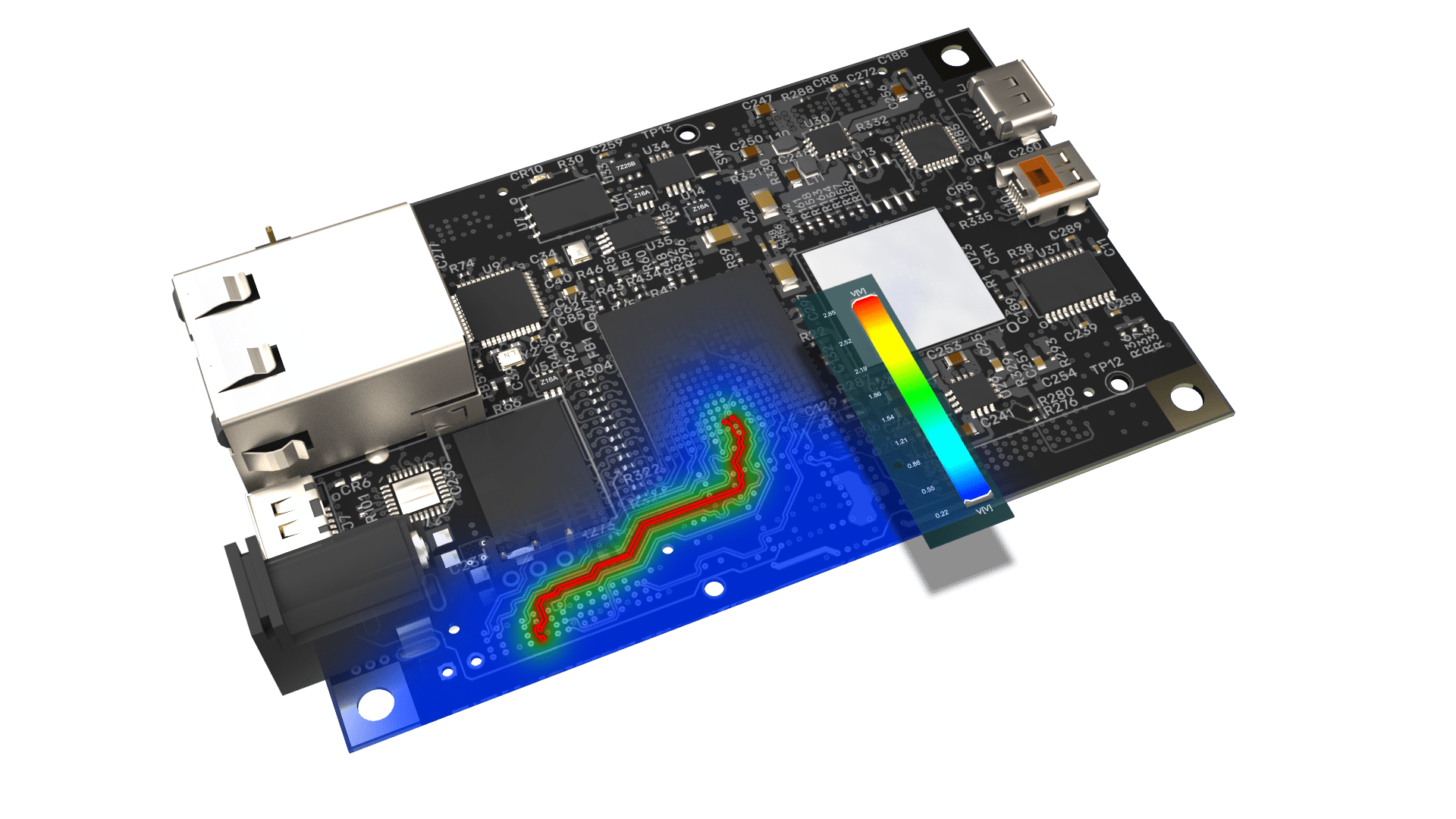
A key implication of this field-based view is the close relationship between SI and PI.
Every switching event inside an integrated circuit requires energy. That energy must arrive within a time frame set by the switching edge rate and propagation delay. If local energy is insufficient, the resulting transient disturbances can affect both signal behavior and power rail stability.
The power distribution network (PDN) delivers energy throughout a system and consists of multiple energy storage and delivery elements:
-
On-die capacitance within the IC
-
Package-level capacitance and interconnect structures
-
Board-level decoupling capacitors
-
Power and ground plane structures
-
The upstream regulator or power supply
Each of these elements contributes to energy delivery at different spatial and temporal scales.
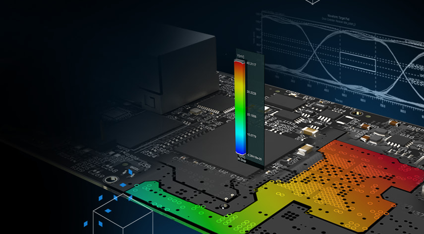
The primary challenge in PDN design is not maximizing capacitance but ensuring sufficiently low impedance across the relevant frequency range so that transient load current can be supplied locally without causing excessive voltage ripple.
The Role of Decoupling Capacitors
Decoupling capacitors are often described as components that reduce noise or filter unwanted signals. A more accurate interpretation is that they provide localized energy storage to support fast transient current demands.
When a switching event occurs, nearby capacitors and closely coupled power-ground plane structures provide energy first because their effective inductance is low, allowing transient current to be delivered quickly. Energy from more distant capacitors and upstream power sources arrive later through the PDN. This leads to voltage fluctuations that affect both signal behavior and power rail stability.
From this perspective, capacitor placement is fundamentally a timing and impedance problem, not only a capacitance sizing exercise.
Distance, Time, and High-Speed Design Constraints
At high speeds, PCB behavior becomes increasingly governed by propagation delay.
Although electromagnetic fields travel at a significant fraction of the speed of light in PCB dielectrics, energy does not propagate instantaneously across a board. A change in load demand takes time to travel through the network, and energy replenishment takes time to reach the load through the PDN.
As switching speeds increase, physical distance between energy storage elements and switching devices becomes a key constraint in maintaining voltage stability. This is why modern high-speed systems rely heavily on tightly coupled power and ground structures and carefully distributed decoupling networks close to active devices.
Ground, Reference Planes, and Field Continuity
Reference planes are sometimes described as “ground sinks,” but in practice they serve as reference conductors that define boundary conditions for fields.
Maintaining continuity in these reference structures ensures that fields remain confined and predictable while helping maintain controlled impedance and low loop inductance. When discontinuities such as splits or poorly managed transitions occur, the field distribution must adapt, which can increase electromagnetic emissions and degrade signal integrity.
The key design objective is not to eliminate current flow in reference planes, but to maintain controlled electromagnetic field paths throughout the structure.
A Unified View of PCB Behavior
A useful way to unify signal integrity and power integrity concepts is to recognize that:
- Energy is transferred by electromagnetic fields in and around conductors
- Conductors define the boundaries of those fields
- Dielectrics are the medium in which energy travels
- Circuit theory provides a valid but simplified abstraction of this behavior
- SI and PI are different perspectives on the same physical system
This unified view helps explain why design rules around impedance control, decoupling, and reference plane continuity consistently improve performance.
Conclusion
Understanding how energy actually flows in a PCB is essential for designing reliable high-speed systems. Traditional circuit models remain essential for analysis, but they do not fully describe how SI and PI behave at modern switching speeds.
A field-based view helps explain why layout, stackup, and power distribution decisions have a strong impact on system performance. It’s also worth remembering that real interconnects are lossy: skin effect, copper roughness, dielectric loss introduce attenuation, while vias, connector, and plane resonances introduce impedance discontinuities that shape how energy actually moves through a board. To explore these concepts further, watch this on-demand webinar to learn how electromagnetic energy shapes signal integrity and power integrity in modern PCB design.