How Do Return Path Discontinuities Create EMI in High-Speed PCBs?
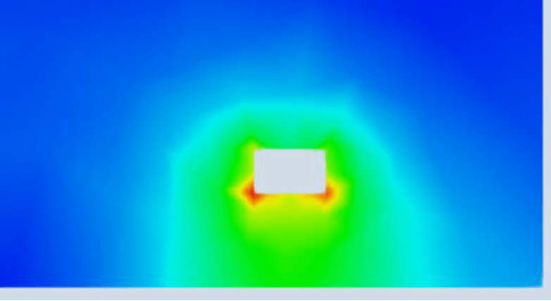
Figure 1. Cross-section view of electromagnetic field surrounding a PCB trace
Every high-speed signal travels as an electromagnetic wave that creates a signal ‘pair’, even when the schematic shows only one trace. There is the primary (or ‘forward’) current on the signal trace, and there is the mirror current on the reference plane right below it.
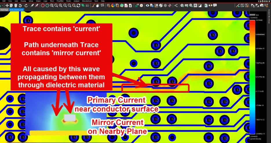
Figure 2. Electromagnetic waves sandwiched between a trace and a nearby plane
The electromagnetic waves and fields propagating through the PCB dielectric and air, guided by the traces, will form a looping area, guided by nearby conductors. Or the wave propagates through the dielectric then eventually out to free space (another dielectric). The shape of that area determines whether your board passes the compliance chamber or fails it.
When the reference plane stays continuous beneath the trace, the loop is small . When the reference plane has a gap, a split, or a layer change without a stitching path, the electromagnetic waves go anywhere they please, coupling to any conductors it finds, thus creating paths (normally called a loop area).
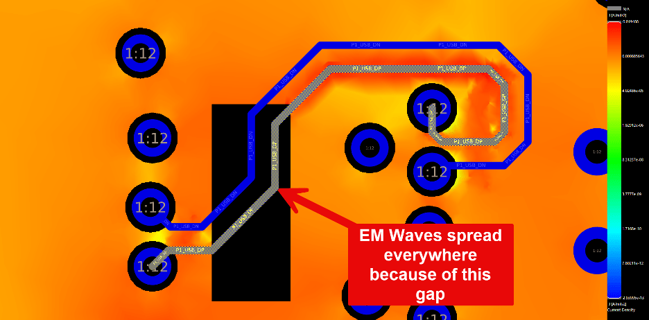
Figure 3. A 12-layer PCB with signals on Layer 9. Mirror current shows up on Layer 10 (Ground Plane). Gap introduced on layer 10, showing zero mirror current immediately around the gap.
A bigger loop means more inductance, more voltage ringing at edges, and more radiated emissions. Same trace, same constraints, same DRC. Different reference plane behavior, very different EMI result.
These effects become significant when signal edge rates fall below 1 ns or when harmonic content extends above 100 MHz. Below those thresholds, return current behavior is dominated by resistance and the effects described here are negligible. Above them, reference plane continuity becomes a primary EMI variable.
Why Mirror/Return Current Concentrates Under the Trace
At all frequencies, the electromagnetic waves spread out across the reference plane and take the lowest impedance path back to the source reference voltage (0 V, typically referred to as ground, albeit a misnomer. The term is a misnomer because in a real PCB the reference conductor carries displacement currents and is never truly at zero potential across its surface, but the convention is standard and used throughout this article).
Z=R+jX = R+j(2πfL + 1/(2πfC))
At low frequencies, resistance dominates (frequency, f → 0), because there is minimal inductive or capacitive reactance being induced by the waves. This results in the subsequent mirror current showing up along conductive paths that follow the lowest resistance path (because that’s what dominates impedance).
At high frequency, things change.The waves concentrate directly beneath the signal trace and so does the mirror current as a result. Because that is now the path of lowest impedance , dominated by inductance rather than resistance.
It is a consequence of how electromagnetic fields couple between a signal trace and its nearest conductive material (typically a reference plane). The faster the signal edge, the more tightly the wave, and thus, the mirror (return) current locks itself beneath the trace.
Howard Johnson describes this in High-Speed Signal Propagation: when the return current encounters a reference plane gap, it cannot just teleport across. It has to detour. In a differential pair, this detour creates a U-turn pattern where both return currents redirect inward to find a path around the gap, generating a small current loop that radiates like an antenna in the space between the original and new reference layers.
The size of that loop is what matters.
Three Mirror (Return) Path Failures That Drive EMI
Understanding that the waves and fields dictate where the currents in conductors appear, we can easily predict what will happen if we pay attention to those waves, regardless of routing geometry. When we make routing decisions that cause the electromagnetic field to spread in places we didn’t plan out, the effects can be at best problematic. Here are some decisions that cause EMI failures:
1. Routing across a plane split. A trace crosses from one region of a split power plane to another. The split was created on purpose, often to separate analog and digital power, or to isolate two different supply rails (which I never recommend doing, unless galvanic isolation is a specific design requirement). The signal trace will pass the design rule check just fine if the geometry is valid. The wave, however, hits a wall at the split. It has to detour all the way around the split or jump through whatever capacitance exists between the two plane regions to find a suitable zero reference (return) path of lowest impedance, thus creating mirror (return path) waves wherever that path is found along the way. This behavior adds a field loop area .
Stephen Hall shows this in Advanced Signal Integrity for High-Speed Digital Designs with a TDR measurement of a 65-ohm microstrip crossing a 25-mil reference plane gap. The gap appears as a clear inductive spike in the time-domain response. The loop area grew, the inductance grew, and the signal saw the gap as a discontinuity even though geometrically nothing changed about the trace.
2. Layer transitions without a return path via. Let’s say a signal drops from layer 1 to layer 5 through a via. The signal current follows the via without issue.
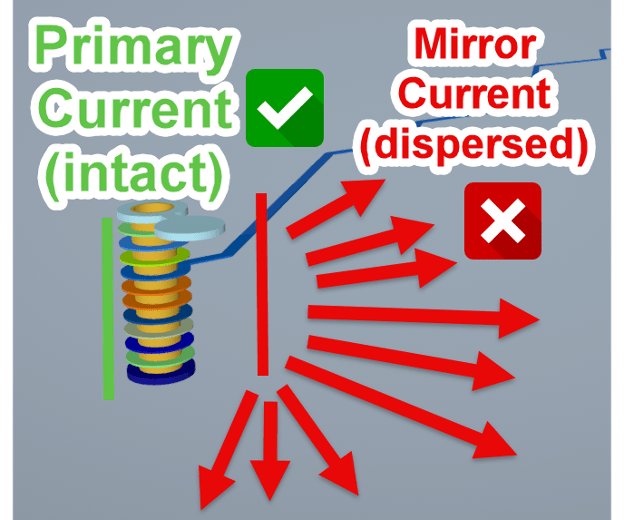
Figure 4. Transitioning layers without a return ground via. Field disperses during layer transition.
The mirror (return) current cannot. It was traveling on the layer 1 reference plane, and now it needs to get to the layer 3 reference plane. If there is no nearby stitching via connecting those two planes, the field, which shapes the current, has to find the next-nearest path, possibly inches away. That detour is the ‘loop area’.
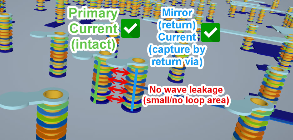
Figure 5. When you add a return path via during layer transitions, waves are contained (red arrows), thus minimizing the ‘return’ current or loop area.
This is the single most common return path failure in real boards. The fix is a ground return via placed immediately adjacent to the signal via, connected to the reference plane that both the source layer and destination layer share. One via, properly placed, drops the loop inductance from inches to thousandths of an inch.
3. Voids and antipads in dense via fields. Below a ball grid array (BGA) or in a heavily routed region, the antipads around signal vias overlap to form a Swiss cheese pattern in the reference plane.
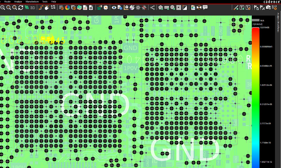
Figure 6. Vias under BGA chips, revealing a Swiss-cheese pattern on a PCB ground plane
Each individual antipad is allowed. But together, they remove enough copper from the plane that return current can no longer find a clean path under any of the signals routing through the region. The remaining copper acts more like a series of narrow bridges than a continuous reference plane.
Staggering vias and managing antipad clearances at the constraint level keeps enough plane intact for return current to flow.
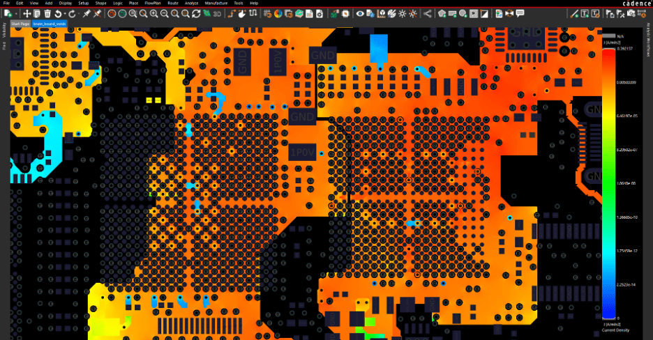
Figure 7. Sigrity X Aurora Visualization of current density in PCB. notice density increasing due to vias from the BGA
How These Failures Show Up
The same physical mechanism creates three different symptoms depending on where you measure it. On a time domain reflectometer (TDR), it shows up as an inductive spike at the discontinuity location. On an eye diagram , it shows up as reduced eye opening and timing margin loss. In an electromagnetic compatibility (EMC) chamber, it shows up as common-mode current radiating from board edges and attached cables, often as a narrow peak at the frequency where the loop happens to be a quarter wavelength.
The board passes DRC. The board fails the chamber. The reference conductor is the reason.
What to Do About It in Layout
The first defense is stackup design. A four-layer stackup with two internal planes that are stitched well together gives every signal layer an adjacent reference and a 3-dimensional reference structure (ground). A stackup that puts two signal layers next to each other (without a plane between them) starts you in a hole that no amount of routing care can fully recover (unless you route ‘ground’ nearby signals on the same layer).
The second defense is routing discipline. Do not route across plane splits or gaps when you can avoid it. When you cannot avoid breaking the field containment, drop a stitching capacitor close to the trace crossing the split. Capacitor value should be selected based on the signal frequency range: a 10 nF capacitor in a typical PCB stackup reaches self-resonance below 50 MHz and becomes inductive above that point. For signals with significant harmonic content above 100 MHz, values in the 100 pF to 1 nF range are more appropriate. Verify the selected value against the capacitor manufacturer's impedance versus frequency data for your specific package and mounting geometry. When the references on both sides are the same net (both ground), a copper bridge under the trace is even better than a capacitor.
The third defense is via discipline. Every signal via that changes reference layers needs a ground return via placed within a few trace widths. Allegro X PCB Layout has a Return Path Vias command that places these automatically with configurable angle and spacing.
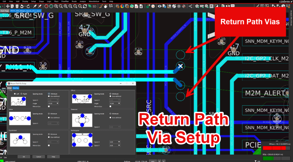
Figure 8. Allegro X PCB Layout Return Path Via Setup dialog and inline placement option selected in the NVIDIA Jetson AGX Orin Carrier Board
How to Verify Before You Build
Waiting for post-route simulation means the design is already complete before you know whether the return paths are clean. By that point, fixes require rerouting finished sections, updating the stackup , or adding vias in areas that are already congested. I find it more effective to run return path analysis continuously during layout rather than treating it as a final verification step. Route a section, check the return paths, fix what needs fixing, and continue routing. Sigrity X Aurora supports this because it reads the Allegro X database directly at any point in the routing process, not just at completion. The color-coded canvas overlay shows return path quality on the copper that is actually there, and jumping from a flagged violation to its location in layout takes one click. Problems get caught when the board still has room to fix them.
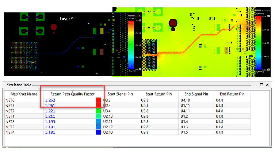
Figure 9. Sigrity X Aurora Return Path Workflow canvas vision showing color-coded return path quality.
You see the problem in the layout, fix it in the layout, and verify the fix in the layout. The compliance chamber never has to find it for you.