Maintaining a Schedule When Everyone is in a Panic

Image credit: massivesoftware.com Go-Time, run for it!
Progress is little more than a result of steady pressure to move forward with a plan. We are always pushing a plan. Steady progress keeps the wheels turning. Progress plays out in the PCB industry in the form of more robust hardware that can execute code fast enough to keep everyone happy. But that happiness threshold that keeps moving out. More information has to flow for a richer user experience. The bar has been raised over and over to the point where the customer is expecting to be amazed by the product right out of the box.
Keeping the unhappiness-producing glitches at bay has been an ongoing pursuit. The customer expects more and better content with each new generation of today’s devices. The pace isn’t leveling off, either. If anything, the march of progress is in the middle of a massive revolution where a matter of hours decides the time-to-market winner.
Not only are things improving, but the rate at which they are expected to do so is also ever-increasing. The Maker movement and all of the lean/agile development process activities that are in fashion these days ensure that the slow actors will not thrive. The continuous improvement on shrinking timelines puts a greater strain on research and development teams. Taking advantage of small process improvements can add up to a successful project.
Start With a Plan
The saying goes, “Failure to plan is the same as planning to fail.” There is undoubtedly more to schedule than tape-out-day. It is also certain that no battle plan survives contact with the enemy. What this calls for is educated guesswork up front. Whether the Designer is driving schedule or keeping the Project Manager in the loop, we need to hone the skill of estimating a job accurately and with sufficient wiggle room.
The stress comes in when we look back on historical data and say, ‘project X looks just like this and it took six weeks when we planned for it to take three.’ Everyone bought into the three-week plan up front except for maybe that cagy veteran board designer who has seen this same thing a few times. Some guru (small g) wisdom: Nobody wants to hear that kind of truth. A little diplomacy will help.
So three weeks go by and the mechanical outline is almost there; except for the crucial connector region. The schematic is done; but we’re still looking for a better version of … Yeah, ok. The schedule is not a cut and dried document. It lives from day-to-day as it reflects the process in real time. To be blunt, a static schedule leads to a surprise ending, and a surprise ending is something else that nobody wants.
We do the best we can to meet the marketing window knowing that a schedule slip can make the entire effort add up to an expensive exercise in futility. But effective communications will get you out in front of the problem early enough for the Marketing team to push back customer samples one week. Good on you. And what a week! All hands on deck for a seven-day slog. Four weeks is an improvement on the six of last time so maybe some lessons learned provided a leg up. Meanwhile, the takeaway is that the bar is three weeks and it’s on me to execute.
Does it Have to be That Way?
Would anything get done if it wasn’t for the 11th hour? Count on a rush. We’re mainly trying to smooth out the workload. Most schedules start out with the ideal case though it rarely plays out like that. We’re good but, not perfect. We stumble over missing and incorrect information. We rip up blocks of routing that looked great just ten minutes ago. That cannot be helped, so it is wise to take a philosophical approach. I like doing the placement and routing, but I want to detach from the whole deal and be ready to react to new information even to the point of blowing the thing up.
The path to a completed PCB is a zigzag every time out, and every one of them is different. Charting the actual course and comparing it to the proposed timeline after enough projects is where I get the idea that we’re usually given about half of the time we actually require. Becoming more efficient with our time and the tools is our best defense against stratospheric expectations.
Own Every Problem
It doesn’t matter where it came from, all PCB design problems are our problems. As long as Management knows that you will keep them in the loop with solutions to problems and schedule impact estimates, you will get the latitude to do the work you need to do. If you find that this is not the case at your current job, be open to offers. The job market is hotter than a solder pot right now; problem solvers needed.
Codevelopment towards a moving target on a static schedule is a recipe for anxiety. Most of us keep our head down and grind it out as best we can. Spending a little of that design time on managing expectations will make life easier. On that note, own your mistakes personally but stick to describing how you will work around obstacles without assigning responsibility for those things beyond your control. Anything that gets kicked down the curb will be there at the end and looming larger, potentially beyond containment.
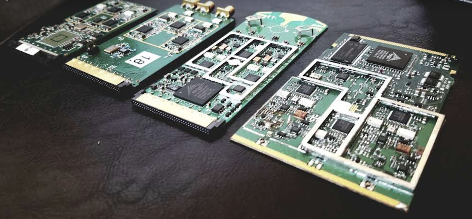
Image credit: Author - the shrinking WIFI router
One case that was beyond my control was when the team was tasked with designing three interrelated boards. The novelty was getting all three sets of artwork tapped out on the same day. This was a red flag for so many reasons. A mid-stream improvement to one board would be a reset to the others. The notion of sending multiple boards out for a quote on the same day can clog the front end of the fab house and all the way down the chain.
A vicious cycle of edits coupled with having three boards in their eleventh hour of development made me nervous. Anything that could be scripted and reused from one SKU to another was on the table. Everything that could be done to clear the slate had to be pulled into the early part of the timetable.
Some of the ways we can leverage work on variants of a PCB done in parallel
-
Same electrical, physical and spacing design rules
-
Reuse keep-outs and other portable constraints
-
Dimensions, notes, and details that are common on fabrication drawings.
-
Check your library footprints - again! My guess is that this is the number-one cause of scrapped boards.
-
Cleaning up the silkscreen and assembly reference designators. It will always take a second pass but it is a serious leg up to have 80% of the text in the correct location when the time comes.
-
Panel drawing, solder paste stencil, XY placement approval from the assembly team.
-
Most of all, a mild sense of urgency from the start will mitigate the onset of panic at the end. Attack the job early with the things that have a good chance of sticking around.
You may also have some tried and true design reuse methods that I’ve overlooked. Automation comes in many forms. A checklist is nice but I’m still prone to forgetting something that causes me to re-do the artwork once I’ve had a chance to view it. I recommend at least a quick view of each artwork layer and, if you have the luxury, a second set of eyes on the doc package before it goes out for quotation.
Live to Play Another Day
We all work hard and want to see positive results that will reinvigorate us for the next challenge. That has to be better than burning out from overwork and underappreciation. Steady progress or steady reports on the lack of progress? That is an easy choice that we can make by getting out front of the PCB layout with solid communications and meeting those high expectations or managing them down to a feasible state. Smart work = success.