04 - Controlling Trace Length for Digital Circuits Using OrCAD X and Allegro X Tools
The general rule for routing is that shorter is better. Placement remains in flux as the fan-out and routing goes along. Printed circuit boards of moderate to high complexity will feature groups of traces that are related to one another; generally in the digital realm. These are known as busses or match groups where all of the members are of the same or similar lengths. A good bus will feature net names that indicate the nature of the circuit.
Regardless of its exact name, one member of the group is designated as the target for the rest of the group members to guide their length. The first step is identifying the members and their leader - if one connection is singled out as such. The OrCAD X schematic tool has the same constraint manager as the layout tools so it’s possible for the schematic to carry that data over to the board layout.
We can expect impedance and targets in ohms while it’s up to us to find a way to carry that information to the board as stack-up geometry, line widths and air gaps. The timing budget may be a little more nebulous. The length matching information is often part of a stand-alone spec for a type of circuit, be that DDR, EMMC, SPI, or what have you. You’ll want this information ahead of the placement process as these factors will prioritize some components over others.
We look for labels and notation on the schematic to help define the groups to be matched. There’s always a tolerance to the lengths. Sometimes, the tolerance is vanishingly small. Other times, it’s rather generous. Even so, a lot of people will ask for a better outcome than simply meeting the requirements. It may seem to be over-engineered but to truly match the line lengths will leave enough margin to add a crucial via without derailing the timing budget.
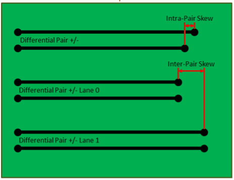
Figure 1. Intra-Pair Skew is set to a maximum of 5 mils for PCIe busses. There is no spec for Intra-Pair Skew although the maximum length of the traces on a board is somewhere between 12 and 15 inches according to app notes I’ve found regarding different generations of the spec. Image Credit Texas Instruments
Knowing the requirements is part of the effort. Depending on which of the four generations of PCIe we’re using, the operating frequency can be 1.25 GHz, 2.5 GHz, 4 GHz, or 8 GHz with data rates at double those frequencies. Yet, all versions have the same amount of phase tolerance.
First, you have to route the signals. Then you can see what you have and react accordingly. When there are differential pairs, I start out by solving for intra-pair skew (phase matching). When both the P and the N length are equal, you get more margin with the inter-pair tolerance. Any length variations between P and N eat into the available tolerance of the pair to pair length matching.
While it’s not a firm requirement for PCIe, there are other buses where multiple lanes need to match up in length. I try to overachieve on length matching. It’s not that hard when you have a meter telling you exactly how much the traces have to meander in real time in order to meet a certain length.
The Computer Says My Trace Is Too Long and Too short. Now What?
That said, it can be tricky to interpret what the meter is trying to tell you. The clock can simultaneously be too long and too short while it might actually be the proper length. What that is telling you is that a member or members of the group are too short to match the clock in its current length while others are too long. If you analyze the match group, the actual lengths are shown in the constraint manager so you can easily find the longest line and work to shorten it. That effort helps the shorter ones get there with minimum jogs.
When a bus is routed but not tuned, it helps to survey (analyze) the actual results before starting the meander process. Highlighting the longest trace(s) one color and the shortest another helps plan the timing resolution. Once a net is length matched to within spec, it could be given another color so you know not to slide that one around. When everything is resolved, the “fixed” property will lock the group into place so it isn’t accidentally edited.
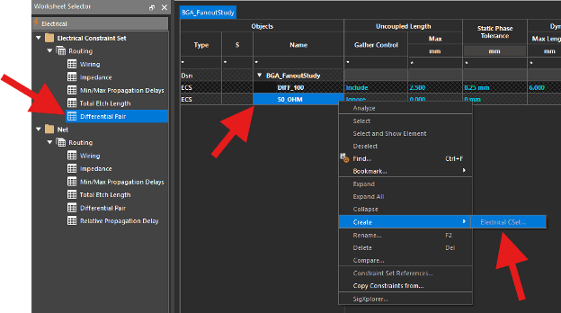
Figure 2. Much like physical and spacing constraints, the Name column is a place for the Right Mouse Click to open up options. Here we're creating a new Electrical Constraint Set (ECS) using the 50_OHM ECS as a template. The general values are set in these upper pages while the nets below are broken out for selection to follow the rules from above.
Adding The Length of Two Nets That Are Divided by a Series Element
Be aware of series resistors and similar components along the length of a tuned connection. See to it that both sides of the series element have a name that would indicate its special use case. The two nets may need to have their lengths added together while others in the group may or may not have a series resistor. If any, the clock needs a buffer.
We call this case an “x-net”; using this feature is part of the Cadence “high speed” routing option along with pin-delay and other features. Another clever use for x-nets is for DC routing when there is a multi-segment loop spanning different nets that must be kept short in total. In order to pass through design verification, the placement will have to be tight in order to meet the routing rules that depend on pin-pairs for their definition.
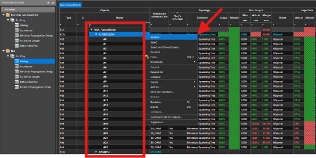
Figure 3. The first net-based constraint assignment covers the ECS selection, Net Schedule, Topology, Stub Length and Layer Set. Here, upon right mouse clicking the Analyze option, we get the full report where it shows some stubs and some wiring on an unauthorized layer. Other electrical constraints will have different analysis options based on their own criteria. In all cases, red cells indicate non-compliance. Again, the filter can hide all but the interesting ones for quicker resolution and verification.
The pin pairs are the way to choose the first and last pins where there are intermediate pins that would separate those two pins into different nets. The example I use is the series element that is inserted in a controlled length line breaking it into two nets that are considered one link in terms of length matching.
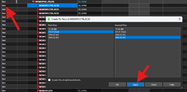
Figure 5. Adding a pin pair is invoked with a right mouse click on a net in the same column as Figure 3. Instead of Analyze, it’s Create > Pin Pair and it pulls up this window where the pins of a net are listed twice for selection as potential the start and end points. Your selection is based on the terminal locations of the net, usually first and last stop. Let’s say you have a diff-pair where one net has a shunt element at the connector where the other net does not. Then, you would Include the endpoints that would allow phase matching without including the stub.
Using Two Match Groups Rather Than XNets
Take a bus where all of the data lines have a series resistor in the path between A and B. If you don’t have the high-speed option and you still want to bridge across the component to find a total length of two nets, it is still possible to automate that to some extent.
The easiest way to do that is to make sure both sides are independently matched. Try strategically placing the series elements so that one side of the connections lends themselves to a natural length matching. If all of them end up routing to a length of say three millimeters, then all you have to do is make a match group out of the nets on the other side of the resistors or whatever is breaking the chains. In terms of maximum length, you still have to account for the 3 mm used for the fan-out to the resistors.
When two nets are used for a connection where the maximum length is provided as a single value, I like to enforce that with the old school Total Etch Length. This is the one electrical property I used before learning about Relative Propagation Delay. In the example above the short lines of the workaround x-net group would be given a Total Etch Length of 3mm on one leg and the rest of the allowable length on the other side of the resistors as they go longer. The issue is that you are sharing the length tolerance between the two sides so try to really nail those 3 mm segments.
Relative Propagation Delay - The Best Tool for Length Matching
Creating a match group will make those nets a candidate for length matching. Differential pairs and single ended traces can become part of a match group. Once a group is established, it is trivial to select or highlight the group as a unit. Then a single entry will allow us to set a rule for the entire group.
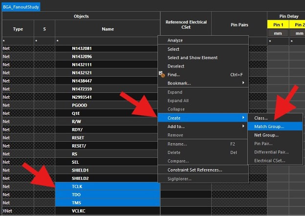
Figure 6. Creating a match group involves selecting the nets and using the right mouse click to create the group in the Relative Propagation Delay window or other electrical net assignment option. Here, we are creating a group of three nets which will be labeled I2C.
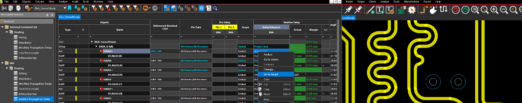
Creating the match group allows us to limit any deviations according to the specification. There isn’t a maximum length for I2C but I added one along with the relative propagation delay which is also arbitrary. The goal is to show two meters on a trace meander in progress. With relative delay, the bounds are set by a single trace length for the others to match.
… make the Signal Integrity people want to have you on their jobs every time.
For the minimum or maximum, a number value is provided as the upper and lower limits. I find the Total Etch Length constraint is helpful for getting into the ballpark where all the traces are between the minimum and maximum. From there, the relative propagation delay rule will help resolve a better length match. You can center-cut the meter so all lines end up essentially the same exact length. This fine tuning along with rounded off corners will make the Signal Integrity people want to have you on their jobs every time.
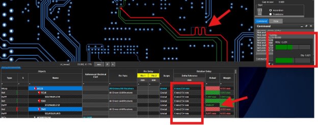
Figure 7. Here, we have created the I2C match group and want to add timing rules. The arrow near top center indicates where a trace (red) is being lengthened to match the two green ones. To the right, you see the meters. A differential pair would have another meter that indicates the status of the phase matching. This one shows a three segment meter for the length relative to the designated clock. In this case, the system selected TDO as the clock. A right mouse click in the Delta:Tolerance column allows us to pick a new clock such as TCLK in this case. Below is a two segment meter that controls the maximum length to a set number. A minimum length can also be applied which helps resolve a match group by providing more context.
This isn’t meant to be a comprehensive tutorial but more of an overview of the constraint manager. We’ve covered parts of the Physical, Spacing and Electrical worksheets. The Same Net Spacing works much like normal spacing but only as it relates to objects of the same net. The thrust of this constraint is to avoid air gaps that are not producible but would not otherwise be flagged as a short.
The manufacturing worksheet is broadly focused on DFx issues. We went over the placement function in the first section. Meanwhile, the fabrication sheet is a way to generate hard-stop air gaps between features. These values are oftentimes straight from the fabricator’s capabilities literature. The idea is that these are a baseline minimum while there are probably larger air gaps in play for other reasons. The DFM rules are more of a backstop, an ultimate limit. The actual spacing rules will hopefully be more conservative everywhere except within special regions for HDI or UHDI.
The reader is encouraged to poke around. The scope here is to shed some light on the constraint manager to get you going. There are deeper dives on the Cadence website and in Help documentation along with useful videos on YouTube that provide easy wins when you need to know how something works in detail. It takes some doing to set up constraints but the reward is in how efficient it becomes to deliver compliant PCB designs on time. When it comes down to crunch-time, a good set of constraints will guide you to the hoped for result; a win.
If you have any questions or comments about the OrCAD X platform, click on the link below.
Contact UsClick here to download the PDF.