Getting the Edge on Design For Test
Building a Printed Circuit Board that works as intended is only has hard as you make it as a designer. The truth is that the layout can be a source of success or failure. Most of the features in the CAD software are geared towards avoiding failure. Going above “acceptable” and gearing up for success in the face of a competitive market is a value add that a test-minded PCB Designer can deliver.
In Circuit Test
Continuity testing can be done by probing a bare printed circuit board. More information is gathered by functional testing of a populated PCB assembly. Buzzing out the bare circuit or probing a device under test conditions is time-consuming and not always able to capture the full picture. The “holy grail’ for test technicians is 100% ICT coverage. ICT stands for In-Circuit Test. The fixtures can be costly, especially as the test point size and pitch is reduced. This is a technology best suited for roomy boards.
The upshot is that every net on the PCB can be accessed by a test fixture called a bed of nails. As the name suggests a number of so-called pogo-pins are spring-loaded and arranged in the same pattern made by all of the test points that were set into the copper by the board designer.
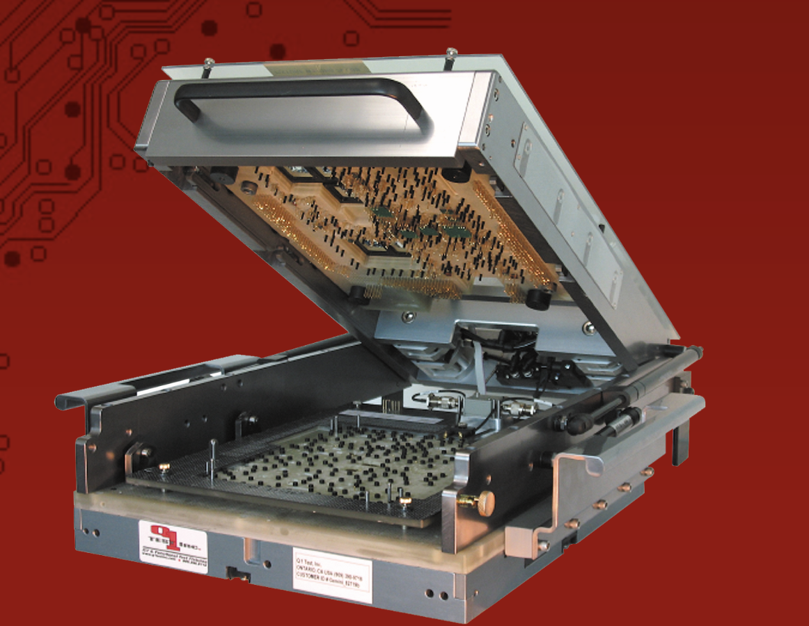
Image Credit: Q1Test a bed-of-nails clamshell tester capable of probing top and bottom.
There are rules as to how close the test points may be located with respect to each other and to components, especially tall components. If you could somehow arrange all of the test points on a perfect grid spaced evenly across the top of the entire board, the test people would love you. That’s pretty unlikely to happen so just bear in mind that too many in one small area will start to deform the board while it is in the fixture.
Flying Probe
A flying probe tester uses a pair of robotic arms to perform point-to-point testing using the same test points. Being programmable makes it quick and cheap to deploy. It tests sequentially rather than all at once so it takes longer and slices up the data accordingly. Flying probe fixtures are most useful for pre-production testing.
As you don’t want any unnecessary stubs on an RF line, the test point becomes a part of the placement strategy. Don’t be surprised when the RF expert tells you unequivocally to get rid of them. While it may not be a stub, a test point is larger than a typical 50 Ohm trace width. A wise solution is to have it both ways. A thick enough dielectric will necessitate a wider trace that engulfs the test point. The trace is also about as wide as the 0402 blocking cap so that is a bonus in terms of discontinuities. Micro-vias and HDI stack-up considerations are the main reason more boards are not like this.
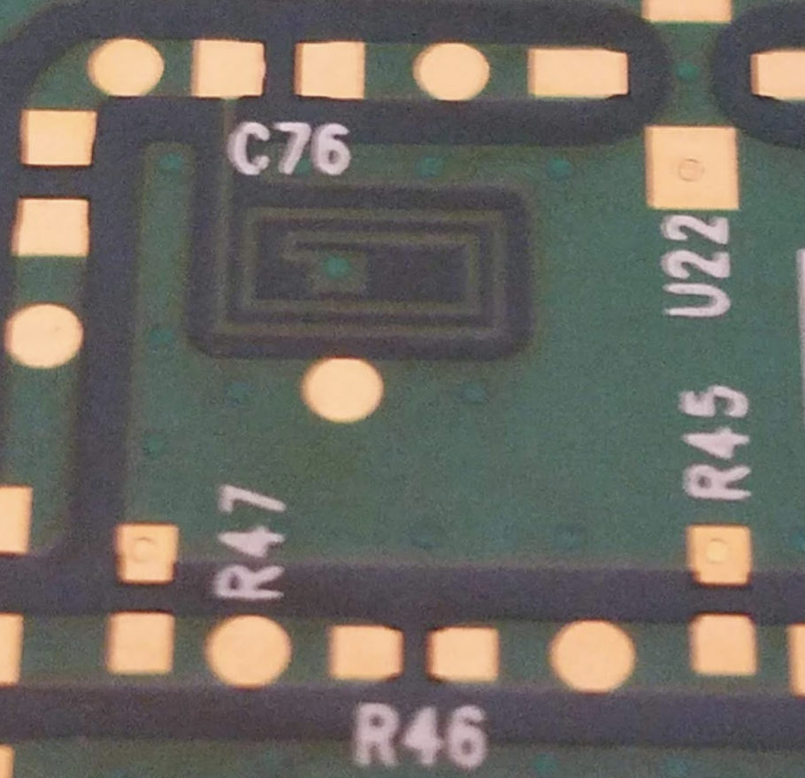
Image Credit: Author - Starting with space for ICT is the easiest way.
The overall footprint of the product may not shrink much but the area designated for the printed circuit board sure does. Make way for bigger batteries while adding some other thing that makes the product more appealing. Features creep into a design and usually have to be supported in future iterations.
Are we going to get a new USB connector every four years? I still use type A for the thumb drive, micro-USB for a Bluetooth speaker and my favorite example of overkill tolerances, the Type-C for the phone and laptop. My rant about them is available somewhere so I digress. Bring on Type-x.
Burn-in
Burn-in is a process where a finished product is subject to thermal stress. A number of test subjects are put on a burn-in rack that has all of the necessary electrical outlets to power up the units. On a small scale, the rack is part of a small oven. Scaled up, a multi-shelf rack is rolled into a burn-in room.
The idea is to certify that the product can last the length of the warranty or otherwise accomplish its mission. Aerospace and similar applications would have you stress testing some units until failure. A scenario could be running at 80% of the maximum rated power while enduring temperatures just below the Maximum Operating Temperature. The temperature could also be cycled to simulate days at 10x the usual time scale. Early aging in salt-fog, as well as shock and vibration tables, are put to use.
The power could be modulated to various “corners” where one worst-case attribute meets another. Let’s say that the 3.3 Volt supply is barely up 3V while the 5V is closer to 5.4V, not to mention the 1.8 or even lower voltages where a little variance or noise can have severe consequences. So a multitude of factors can be analyzed against one another. A good test protocol is going to take every voltage domain into consideration; more regulators equal more corner-case testing.

Image Credit: Abrel
Most of the time, stress testing is not meant to destroy the product. 100 pre-tested units go into the chamber for 100 days and then get retested to see if there is any degradation in performance. Lessons are learned from the early failures and customers live a more peaceful existence knowing that you (as a company) are on the job making the product safer. In telecom, it went beyond a sample. All of the printed circuit boards went through burn-in. Only a few were left in there to see if it would fail over the long term.
Often, a JTAG or I2C interface may be all that’s required to monitor devices under test. The equipment includes a permanent record of the temperature readings and so forth. Establishing the history of all of the products for traceability falls under the guise of continuous improvement.
We should be doing that whether our customers mandate it or not. As a corporate culture, the minute we stop thinking about the future is the minute we stop having one. Including testability in our early planning stage gives us the chance to continue the journey down the road.