Mixed Signal PCB Design Techniques
Mixed Signal PCB Design Techniques
The analog world in which we live is constantly being captured in one way or another, and the media is being shared globally. In between the creation and consumption of all of this data, the information is converted to digital representations of itself for storage and transmission. Standard, live radio and television broadcasts are done with an end-to-end analog chain. That technology has become an evolutionary cul-de-sac as digital protocols have taken the traffic to levels that are unreachable with analog equipment.
I first became aware of this trend when the U.S. Government broke the American Telephone and Telegraph (AT&T) company into a collection of "Baby Bells". Suddenly, MaBell, PacBell and all of the others needed new office equipment. We're not talking about printers and FAX machines. We're talking about one of the most significant turning points in telecom history. For about a century after Mr. Bell's invention, a network of switches and wires was built across the land.

Image credit: Vanalog Files - the sky is darkened by the wiring.
The so-called T1 or Plain Old Telephone System (POTS) was good enough. One twisted pair of wires could accommodate 24 individual phone calls. Build a sub-division and bury a bundle of twisted pairs. Build a metropolis, and the wires go everywhere. Geometric growth of the cities finally became more than the POTS could handle. The S.F. Bay Area was already leaning away from agriculture and towards technology when the revolution started. While AT&T was taking one of the biggest write-offs ever, the entire analog phone system was not actually being scrapped.
A local start-up got into the game with racks stuffed with PCBs. The racks were called Trans-MUX and featured some heavy duty Digital to Analog and Analog to Digital Converters; among the eight cards that made up a group that did the multiplexing on phone lines. The new equipment on the market allowed 384 (Model 3) and then 576 phone calls (Model 4) to be made over a twisted pair rather than the old limit of two dozen simultaneous calls. Since the old pipeline was now digitized along the city-to-city trunk lines, moving data was the natural follow-on application. What a monster of an application. Fixing the phone system gave rise to the internet. It is that simple and that profound.
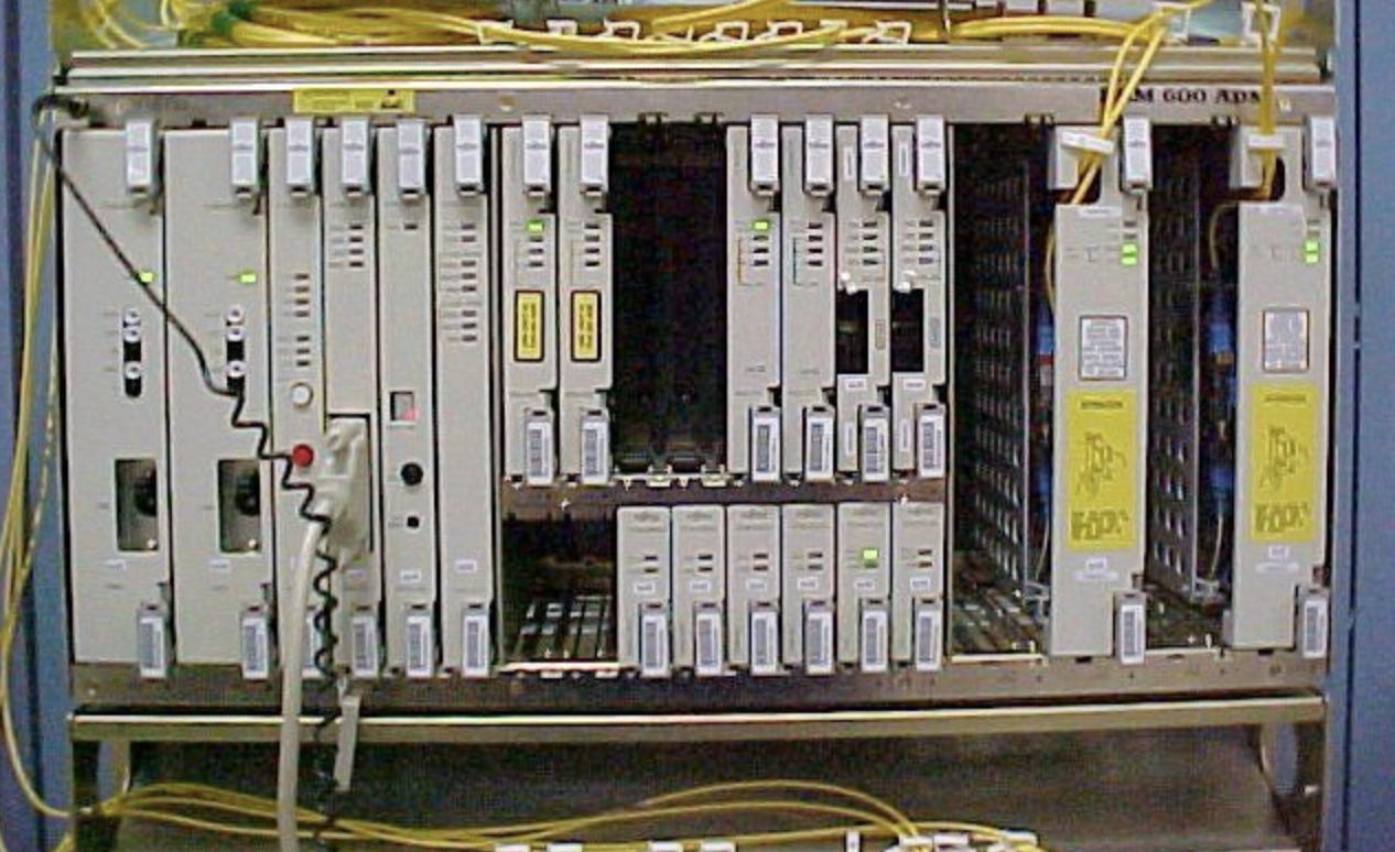
Image credit: Fujitsu - a competing multiplexer of the period.
You do not have to reinvent telecommunications to appreciate the value of converting sine waves into a bit stream. We did it again with the cellular revolution. By then, I was designing correction boards for RF amplifiers. Those single and multi-carrier amps lived in the base stations that make wireless phones the work. The correction boards kept the RF devices true to their mission with a variety of techniques. The common thread among the correction boards was to sample the data stream and then adjust the input parameters of the amplifier in some way to keep the magic smoke from coming out of the devices.
Why Stop There?
Another company helped the world move from cell phones to smartphones with the addition of a WIFI router chipset. This was on the back of Qualcomm’s CDMA technology. They eventually acquired the start-up and incorporated the IP into their reference designs. That was my job too. Analog op-amps and comparators lived next to digital signal processors. The further we could get those digital parts from our analog ones the better. Whether it was by using the top and bottom of a double-sided board or the left and right side of a single sided layout, space is the mixed signal designer's best friend. When forced together by form factor, we would be more willing to compromise the transmit chain than the receiver. The thought here is that the receive chain is a lower energy transmission line and thus, more susceptible to errant noise. Then the amplifier gets the noise and does what an amplifier does.
The Usual Suspects
Where, precisely, does the noise come from? Mostly from oscillators (crystals) or clock lines but the electromagnetic fields around big inductors and switch mode power supplies are also notorious sources of interference. Big voltage swings of any kind are going to be a problem unless the device that is pulling the current has all of the necessary capacitors, ferrite beads, diodes, and even termination resistors placed and routed for minimum loop length. The loop length is the total path from the source of the power to the load and back to the start by way of the ground plane. Smaller loops circulate around the device and its constituent passive parts.
All of that energy doesn't just sit there. It is attracted to any nearby metallic objects such as a printed antenna. That's why we go bonkers with ground vias around the antenna(s). The antenna itself is often printed on an outer layer with all other layers below voided of copper. The voids also remove a lot of the stiffness that the inner layer metal would have provided. One 12-layer board lost almost half of its thickness due to missing 11 layers of metal. The little spots of copper we call thieving are not conducive to the antenna doing its thing, so we live with a flimsy corner.
It does not have to be called an antenna to work like one. Interference from one device can get into another by coupling in ways we can not always predict. While simulation tools do a good job of characterizing a transmission line, there are gremlins with each device. The more features we have, the more ways things can go wrong. Smartphones are the worst thing I can think of in terms of different ways to fail. A tiny footprint with a new feature added every generation. People think of these things in terms of apps, but a lot of the features have to be fleshed out with hardware.
Bluetooth, GPS, WIFI, NFC and those types of things each get their own device or bit of real estate on a combo device. The radio chips are not suitable for the process nodes of the latest baseband chips. The microcircuits for analog are orders of magnitude larger than those for digital circuits. It seems like we will always have devices competing for space, power and breathing room.
Give Peace a Chance
The best answer for coexistence is to separate the analog blocks using shielding. There are drawbacks. Shields take space in three dimensions. They have to be removed for rework. They trap heat unless the top is perforated. Any shape beyond a rectangle will take some engineering, and there is a significant cost in any event. Additive manufacturing where we can print metal on plastic and/or incorporate EMI shielding with the product housing may be the next idea in isolating the victims from the aggressors.

Image credit: Microwaves & RF - dated but still useful view of typical shields
Isolation requirements can be daunting. Qualcomm's application notes for the latest Snapdragon chip specify 100 dB in some cases. If that was in the frequency range of human hearing, it would be like a passenger jet going right over your roof without anyone noticing. That would be a very robust roof to make someone unaware of a jet taking off overhead. A quieter jet may also be part of the equation. A lot of the new resistors, capacitors, and regulators added to the second revision of a board are there to help the different devices play nice together.
Differential pairs act like the twisted pair of wires in the phone cable. They are much better at rejecting common mode noise than single-ended transmission lines. Clean routing with a minimum number of layer transitions, minimum length and as much space as available will go a long way towards quieting the aggressors. As you may have gathered, some of the same sound design practices will provide the victim traces with a thicker skin to ward off the harmonic disturbances in their vicinity.
A Well Grounded Philosophy
We can't have an overview of mixed signal routing without acknowledging the ground plane. It is quite common to have isolated return paths. The telephone equipment had thick copper rods running the length of the racks. They were held in place with the same nylon brackets managed the rest of the wiring harness. It plays out on a smaller scale on the PCB. Individual devices will have all of their bits and pieces grounded together with a shape that is tied to the chassis ground at a single location. There may be several AGND pockets within the overall ground plane. I try to create a moat around the crystals by slotting the ground plane to corral the EMI back towards the parent device. All of these little things add up.
It comes down to the two tenants of coexistence. One is to make less electromagnetic interference in the first place by using strong design fundamentals. The second one is to make the devices more impervious to whatever noise remains in the system. The FCC stickers on compliant devices spell out both of these conditions. Like a good engineer, a good product is both unflappable and on the quiet side. Knowing your way around an analog circuit as well as a digital circuit will be a good start towards working in the space between the two worlds.