On Printed Circuit Board Stiffeners - Making the Rigid PCBs Actually Rigid
When the term “Stiff as a board” was coined, they were not talking about printed circuit boards. Resin, fiber, and copper that make up the typical PCB stack-up are all ductile materials. Laminating them all together in several alternating layers helps a little but a rigid board is only rigid compared to a flex circuit. This article will focus on stiffening the traditional PCBs in an industrial setting.
Looking at FR4 material on a microscopic level reveals two distinct strata. First is the copper which is a ductile metal by nature. Like any metal, it can be tempered (hardened) or annealed (softened) by heat-treating or other methods. The range will remain on the soft side compared to aluminum or steel. The gold that usually protects the exposed copper is even more ductile.

Image Credit: Author - Oversized openings support RF shields that double as stiffeners.
In between the conductors, we find layers of porous and pliable glass impregnated resin. By itself, this material is really wimpy. I found this out by printing an antenna on the top layer of a 12-layer PCB. Aside from the antenna itself, no other copper was allowed on the other 11 layers below the antenna. That corner of the board was seriously compromised. Conversely, flooding copper on every layer adds backbone and reduces the warpage that can affect yields. That is your free stiffener, Faraday cage and heat sink all in one.
High Density Interconnect and High Layer-Count PCBs - Aiming High
Adding up the thickness values in a modern stack-up separating the conductor layers from the dielectric layers is enlightening. Take “modern” to mean high density interconnect (HDI) boards. The reason for the higher percentage of metal is on account of the minimum aspect ratio for a micro-via. In short, the diameter of the microvia has to be greater than the depth. This drives the use of thinner dielectric materials - basically less insulation.
This fabrication challenge has been with us from the start of the HDI revolution. About the best the industry can do is a 1:1 ratio where the hole diameter equals the thickness of the dielectric. More often this is less than that such that the plated hole diameter is around 30% larger than the depth. More metal content and thicker boards relative to the other two dimensions (X&Y) contribute to board stiffness. Taken to the extreme, metal core boards have a slab of copper and they are, in fact, as “stiff as a board”.
Stiffening a Large PCB - An Example From Telecom Equipment
After using best design practices to get the most from the material, there is still potential for the board to flex under pressure. I’m reminded of the backplanes we used in telecom. We had standard 19-inch wide equipment racks filled up with shelves that held the daughter cards vertically like books. One “rack unit” is one and three-quarters of an inch. We had two groups of eight boards plus two 48V power supplies stacked up in 5 RU shelves. Those shelves were installed in racks that were seven to eleven feet high, depending on the customer.
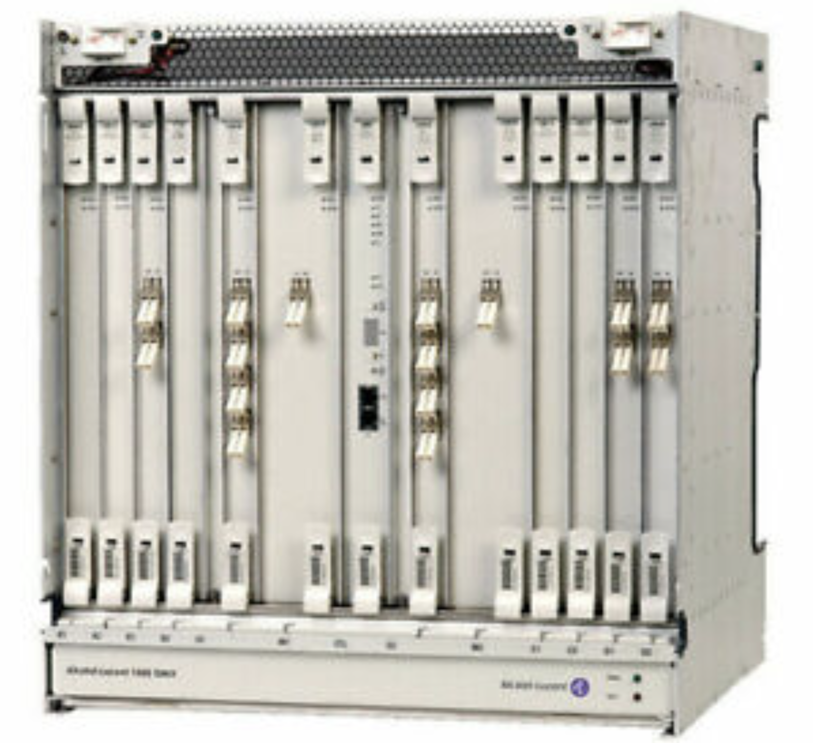
Image Credit: Alcatel - Typical equipment showing enclosures within enclosures and a vent above used as an escape path for hot air
Each of those boards featured a pair of 320 pin connectors on the business end. An aluminum stiffener locked the two connectors in position and bolstered the board along that edge. In turn, the back panel was 19 by 9 inches and was populated end to end with 640 pin press-fit connectors - except where the power supplies plugged in. The yield from one fabrication panel is two boards. When they are that big, they’ll flex under their own weight even if they are twice as thick as typical PCBs.

Image Credit: Amazon - A stiffener mounted to an edge connector where the insertion/extraction flexing stress is concentrated.
The few pins on your phone up little resistance when you engage the charger. PCI cards take a bit more force for their connectors. Multiply that effort by about 50x to engage with the back panel. The front edge of a rack-mount board has card ejector levers that allow you to pry the board out and lever it back in.
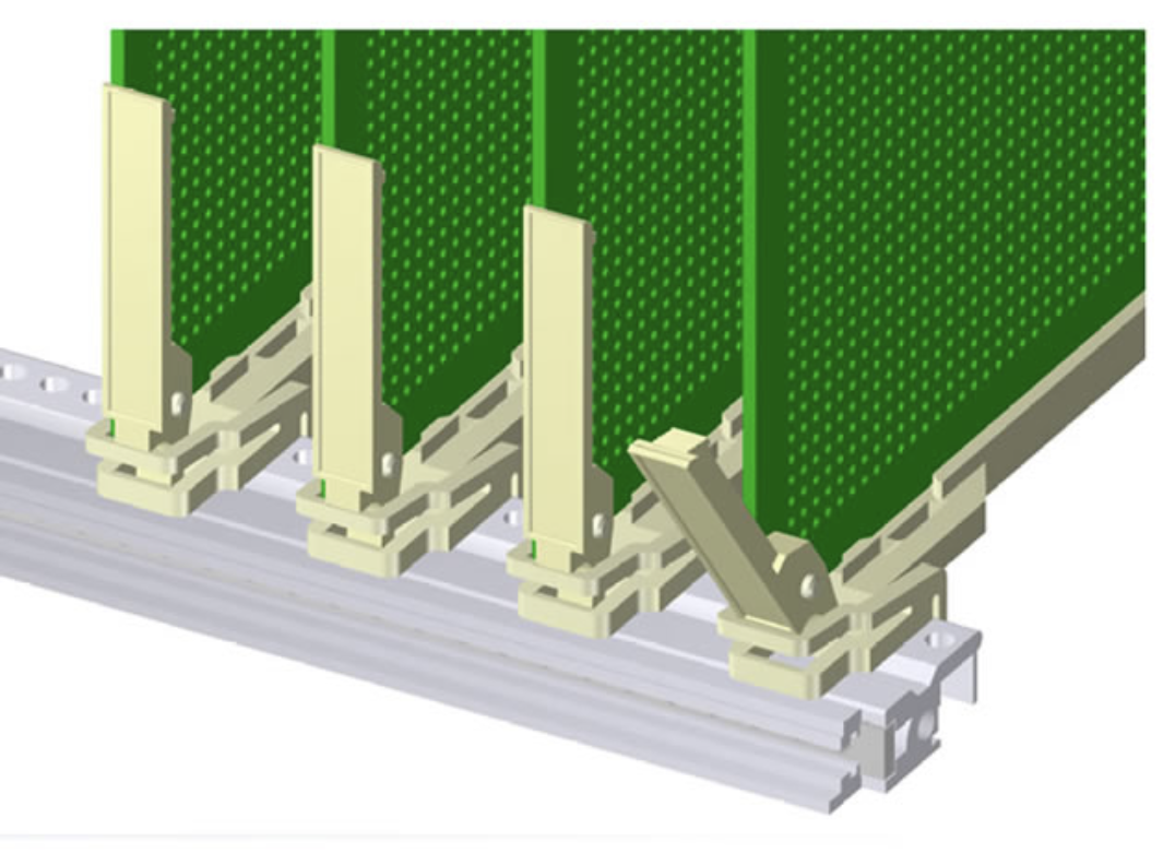
Image Credit: Vector Electronics - The type of card ejector that levers a PCB into its mating connector(s).
That leverage overcomes the grip of the 640 tight fitting pins while exerting tension on the boards. To handle the stress, three aluminum bars are screwed to the other side of the backplane across the top, middle, and, bottom. The stiffener bars also have tapped holes on the other axis that are used to fasten the PCB to the shelf. An aluminum back cover completes the shelf sub-assembly and keeps everything squared up.
Structural Elements Used to Enhance PCB Stiffness
Covers and enclosures do more than keep the dust off of the PCB. The twin demands of the FCC are that your product does not interfere with other products and that it is immune to the noise that does occur in the environment. From a mechanical standpoint, the housing is part heat sink and part structure to keep the board from moving. The size and spacing of mounting hardware will depend on the operating environment.
Automotive and other applications where shock and vibration are expected will require substantially more and larger hardware to keep everything from shaking apart. Busbars, baseplates, sockets, heatsinks, shields and other machined parts can be used as structural elements to keep the PCB in place. One thing to be careful of is a mismatch of the coefficient of thermal expansion. A CTE mismatch can stress the assembly if one type of material expands more than its mating surface over temperature changes. Grommets and gaskets help keep more constant mechanical pressure on the board as it “breathes”. Aim for a firm grip rather than a death grip on the PCB.
Keeping shock, vibration, and other mechanical stresses from affecting the performance of the PCB takes some planning ahead and (usually) some reacting to the surprises as they come. Working with the physical designers, we can solve the mechanical issues that arise in any leading edge PCB production. Simulation and verification will minimize the surprises. Even then, the idea is to fail fast and recover faster while keeping a stiff upper lip.