EDA 101: Schematic Capture and Logical Design
Self-driving cars, smartphones, autonomous drones, and WiFi—these electronic marvels of the modern world would not be possible were it not for advancements in electronic design automation (EDA). EDA (a.k.a. ECAD) refers to the software tools that let PCB designers turn circuit diagrams into integrated circuits (ICs) and printed circuit boards (PCBs). In this post we’re going to focus on the first step in the EDA design cycle: schematic capture.
What is schematic capture?
Every PCB design starts out as a circuit diagram. Remember those universal symbols you used to represent resistors, capacitors, and other components in a circuit diagram?
The process of drawing a circuit and capturing it as a schematic in EDA software is called schematic capture:
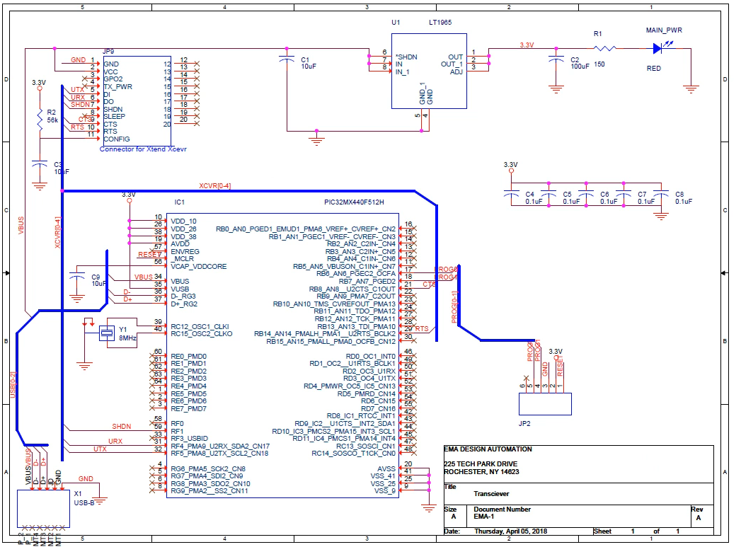
credit: EMA Design Automation
For simple circuits, an electrical engineer will sketch an electronic diagram on paper and then enter the design into a schematic editor, such as OrCAD Capture. Simply transferring a circuit diagram to a computer is only scratching the surface of what a schematic capture tool does for an engineer. Let’s take a closer look at how schematic capture helps with logical design.
Custom symbols, libraries, and interactive schematics
Symbol libraries are the bread and butter of schematic capture. If you already have CAD files for common components, buses, and ICs, you can create your own labels and symbols, and pull them into a new circuit design. Simply click on a symbol to blow it up and view a 3D representation:
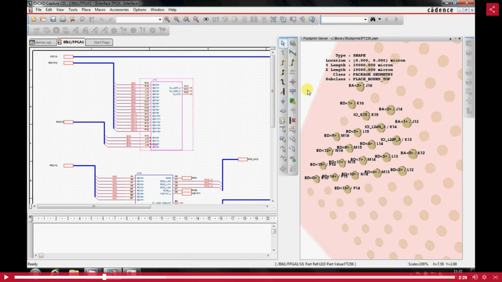
credit: EMA Design Automation
Automated bus routing via net aliases
Autowiring make it easy to route two or more buses together by clicking points. And you can also use net names to automatically connect two points in the design to the same net:
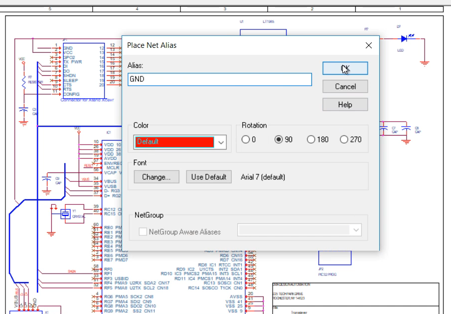
credit: EMA Design Automation
In the above image, everywhere you assign the GND net aliases will automatically be understood to be connected to ground. It is often not feasible to fit an entire design in a single page. This simple net name mechanic makes off-page connectors easy to use.
Schematic capture is crucial for modern PCB design
The schematic capture tool integrates seamlessly with the other tools in an EDA software suite, giving the engineer an interactive, high-level view of their design. With OrCAD Capture you can:
-
Build circuits by linking component symbols together in a schematic diagram
-
Automatically connect two points in a circuit or bus using the autowire feature
-
Link existing components to your interactive schematic.
-
Blow up symbols to view detailed drawings of components
-
Generate smart PDFs and bill of materials
-
Run design rule checks (DRC) to check your physical and electrical connections
In this post, you saw how a schematic capture tool can greatly improve an engineer’s workflow. The demand for faster, smaller, and more robust electronics is likely to continue to rise. Eager to remain competitive in the ever evolving world of electronics? Check out Cadence’s suite of PCB design and analysis tools today.