3D PCB Design With OrCAD X Tools
Key Takeaways
- Factors to consider when designing across complex system assemblies (multi-board, flex/rigid-flex, etc.).
- Performance considerations for different board-to-board connections.
- OrCAD X 3D tools improve design analysis and manufacturability.
3D PCB design for single- or multi-board assemblies helps reduce revision times by checking thermal and mechanical constraints.
A single printed circuit board (PCB) only allows so much functionality. Advances in transistor miniaturization on a single chip have begun to butt up against physical limits. This limitation extends to the system level: with electrical system design more complex than ever, multi-board PCB design is becoming more of a necessity. Supporting a multi-board PCB system design comes with challenges, such as how assembly fills 3D space since the dimensions are no longer bound to an in-plane outline and z-axis stacking. Partitioning and intra-board connectivity considerations play a role in planning a 3D PCB design.
OrCAD X 3D PCB Design Features
|
Cutting Planes |
View cutaway views of the board in any combination of x, y, and z-axes. |
|
3D Material Colors |
Produce photorealistic 3D models by selecting the color of manufactured materials. |
|
Visibility and Transparency Options |
Change layer opacity and visibility of components’ 3D models. |
|
3D DRC Display Control |
See real-time DRC flags in 3D mode. |
|
3D Air Gap |
Measure the air gap between components in 3D mode. |
Partitioning Assemblies With 3D PCB Design
Physically, partitioning involves grouping components based on functionality and nearby circuits (according to the schematic). Each functional subsystem can split into a component and its supporting circuitry. For example, subdividing a motherboard into several functional units, such as the processor clock logic, bus controller, bus interface, memory, video/audio processing modules, and peripherals (I/O), allows more straightforward piecewise evaluation. In the context of multi-board PCB design, partitioning may be followed by placing component groups across different boards. Selective placement of components can yield many benefits:
- Cost - Functional circuits requiring more expensive multi-layer board architectures can be cheaper than those using a smaller board connected to the main board.
- Modularity - Designing multiple products can save a business time and money by incorporating modular, standardized units into a design and adding functionality to a baseboard as needed.
- Enclosure requirements - Given the physical dimensions and shape of the device's enclosure, fitting all the circuitry onto a single board doesn’t always make sense.
Viewing options for 3D assembly is also important, especially when dealing with complex assemblies involving rigid-flex designs. With the 3DX Canvas, OrCAD X Presto PCB Editor users can precisely customize the view options of their 3D PCB model for team collaboration and manufacturing preparation:
- Customizable cutting planes - Users can define any cutaway view with a ± 90° pitch and yaw angle for the x, y, and z-axes and an offset distance slider to move the plane location. The default cutting planes match the six standard viewing sides of the board, and users can combine multiple cuts for additional viewing options.
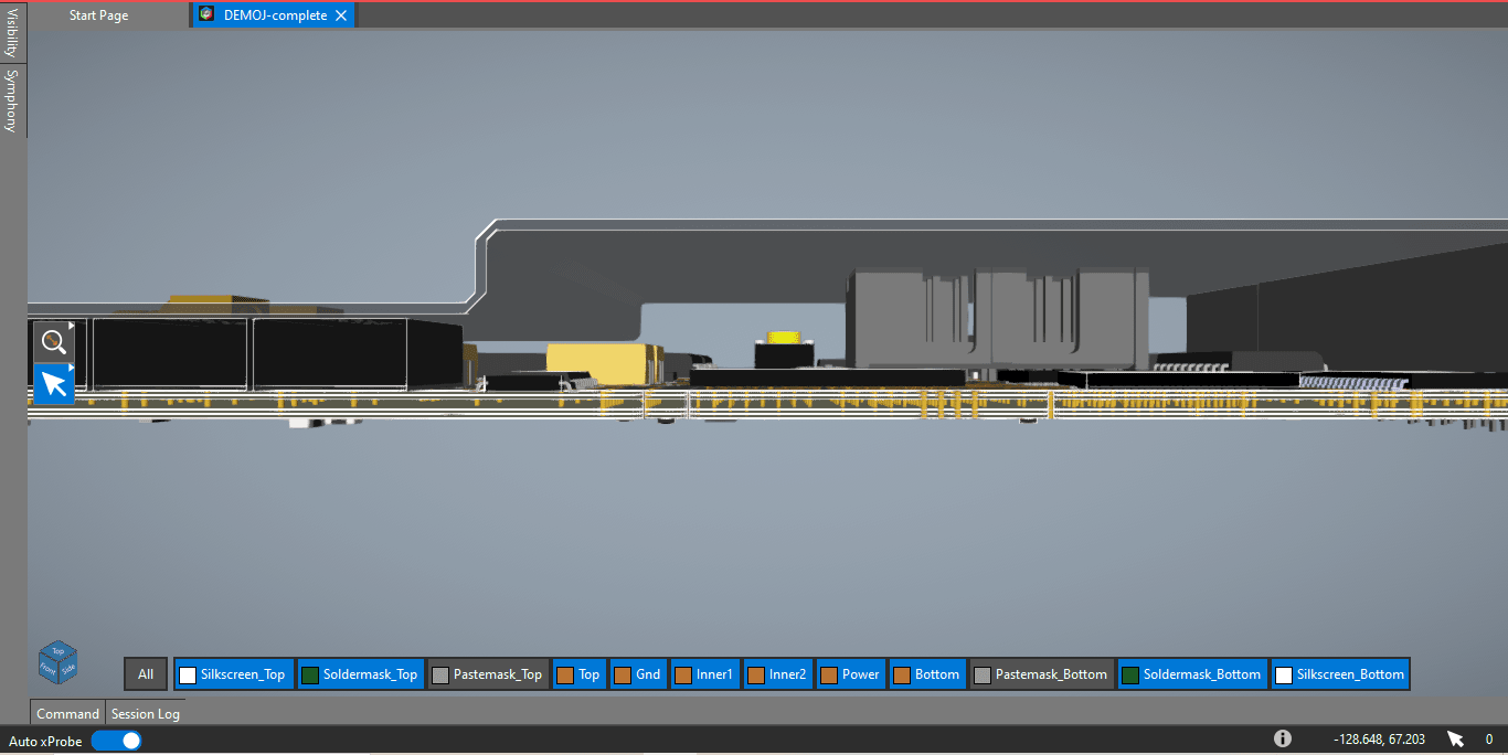
A cutaway of the board shows the internal via connections.
- Layer transparencies - Like with the 2D board design, users can adjust the opacity of mechanical symbols or individual components to emphasize or deemphasize certain board features. They can toggle between full opacity, the global 3D model opacity set in the Display tab, or zero opacity (e.g., transparent). Users also have the option to suppress the model's visibility completely.
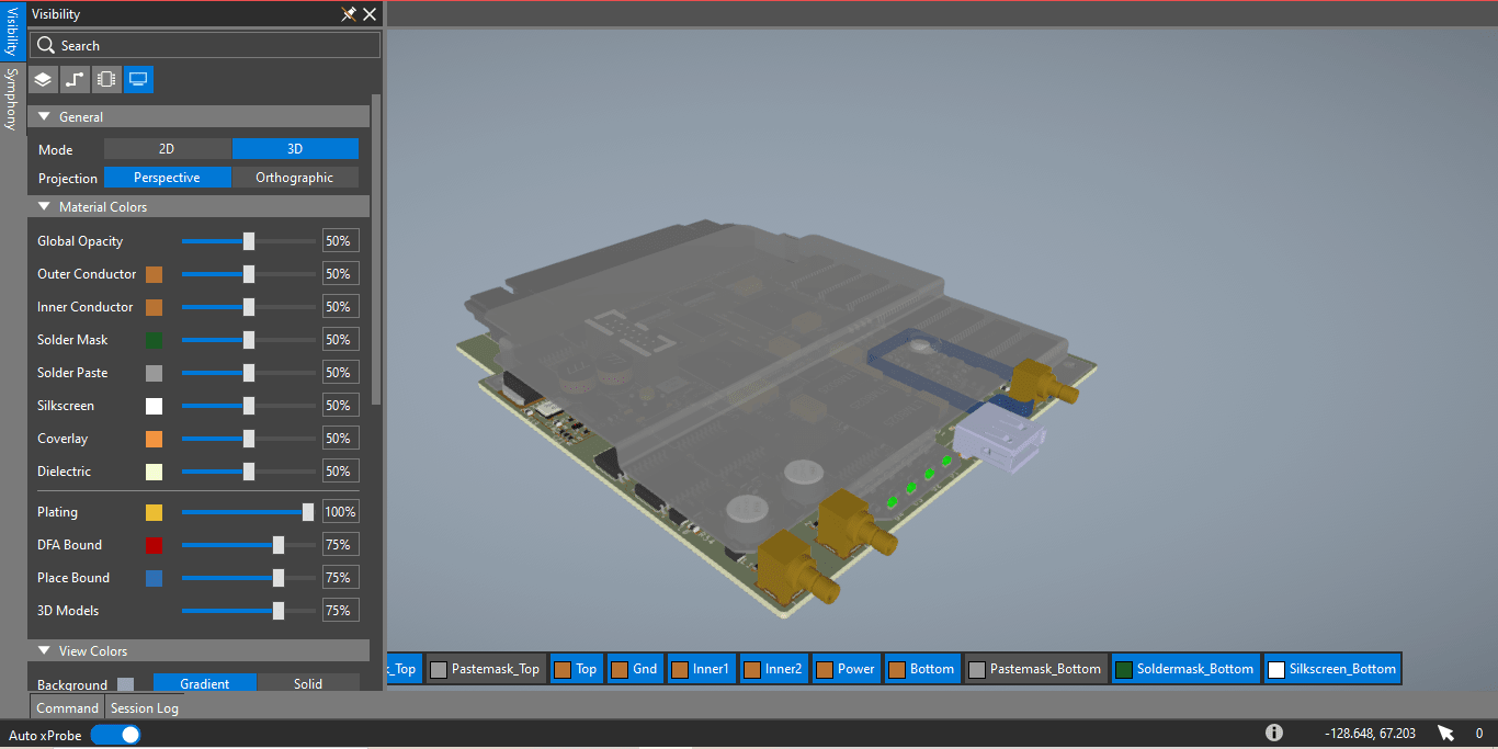
Users can adjust the opacity visibility settings in three dimensions.
- 3D DRC - Users can adjust the visibility of spacing violations (overlaps, spacing requirements, etc.) by changing the color, opacity, and toggling displayed/hidden elements of the DRC flags.
- 3D air gap measurements - By holding alt and selecting a board feature (pad, component, via barrel, track, plane), users will see a line displaying the shortest distance between the two objects.
Electrical System Design and Intra-Board Connectivity
Determining connectors for electrical systems is more than deciding what works best for the production budget. Connectors are multi-faceted and can be make-or-break in some design cases when working through particular power demands. Intra-board connectors serve as the cornerstone of multi-board PCB design. Here’s a quick look at the different types of intra-board connections:
- Board-to-board - Male/female and pin/socket headers are the most common types of connectors. They tend to be low-cost and are impractical for high-speed circuit transmissions. However, you can use higher pin counts and multiple pins to handle larger current draws. A good rule of thumb is to be mindful of the manufacturer’s rated current handling capacity per pin.
- Card edge connector - Traces leading off the edge of one board can mate with a matching socket on another such that the two boards are perpendicular. Card edge connectors often act as expansion slots on motherboards, backplanes, or riser cards, with the PCI-e (Peripheral Component Interconnect Express) slots used to add more RAM to a desktop computer as a prime example. Corrosion-resistant gold contacts that directly contact trace on the board make them great for high-speed digital signal circuits.
- Board-to-harness - In many instances, cables and wires may need to be connected to a board. The prime examples are the FFCs (flexible film cables), FPCs (flexible printed cables), and ribbon connectors characteristic of a server room.
- Direct-soldered - Castellated vias allow you to create PCB modules that can easily be soldered together. These are especially popular for attaching small wireless modules to larger boards.
- Flex - For additional cost and manufacturing complexity, flexible printed circuits can combine the benefits of component assemblies and wire harnesses. Their ductile nature means they can more effectively fill 3D space in small, constrained enclosures.
Whether design requires a vertical stack of PCBs or sliding boards into racks or backplanes, it’s essential to maintain a connection between boards that is neither susceptible to nor an influence on the signal quality of neighboring lines.
Putting It All Together With 3D PCB Design Considerations
Multi-board design is like an expensive 3D puzzle: each board comprising your system must interface correctly and fit into a physical enclosure or case. There’s nothing worse than drafting up the “perfect” CAD drawing and procuring all the materials, parts, and connectors, only to find out on assembly day that the 3D clearances are incorrect. Fortunately, OrCAD X exists to help designers keep track of all aspects of 3D PCB design with a state-of-the-art viewer, DRC, and Constraint Manager that ensure effortless synchronization. Interested in learning more? With PCB Design and Analysis Software from Cadence, users can accelerate design turnaround times for even the most complex multi-board designs.
Leading electronics providers rely on Cadence products to optimize power, space, and energy needs for a wide variety of market applications. To learn more about our innovative solutions, talk to our team of experts or subscribe to our YouTube channel.