PCB Design Parameters With OrCAD X
Key Takeaways
-
PCB design parameters impact performance, reliability, and manufacturability.
-
Key constraints include signal integrity, power integrity, and thermal management.
-
Setting constraints in OrCAD X ensures compliance with electrical and physical requirements.

When you aren’t used to a new set of PCB design tools, the amount of setup that goes into the parameters can seem overwhelming. There are, however, good reasons for all of these parameters, and with the right touch on the controls, your layout tools can conform to your method and style of design. Here are some of the problems these PCB design parameters intend to solve and how you can fine-tune your design environment for maximum productivity by working with them.
Types of PCB Design Parameters and Key Considerations
|
Design Parameter |
Notes |
Key Considerations |
|
Signal Integrity |
Prevent data corruption, interference, and unintended radiation. Signal integrity issues arise due to impedance mismatches, excessive trace length, and improper grounding. |
- Control impedance through trace width and dielectric spacing - Minimize crosstalk by maintaining adequate trace separation - Use proper terminations to reduce signal reflections - Optimize high-speed trace routing for minimal EMI |
|
Power Integrity |
Power integrity depends on proper plane design, bypass capacitors, and low-impedance connections. |
- Design adequate power planes for stable voltage distribution - Use decoupling capacitors near power pins to reduce noise - Ensure low-impedance connections between power and ground - Minimize voltage drop with wider power traces |
|
Board Dimensions |
The overall size and shape of the PCB determine its compatibility with mechanical enclosures, connectors, and other system components. |
- Ensure the PCB fits within mechanical enclosures - Optimize board shape for manufacturability and assembly - Accommodate connectors and mounting holes appropriately |
|
Component Placement |
Placing components based on functional grouping enhances performance and reduces interference. |
- Group related components for efficient signal routing - Maintain proper spacing for thermal management - Position high-frequency components close to their loads - Consider ease of soldering and assembly during placement |
|
Design for Manufacturability (DFM) |
DFM ensures that the PCB layout adheres to the manufacturer's capabilities. Consideration of trace widths, spacing, and hole sizes improves manufacturability. |
- Adhere to manufacturer’s trace width and spacing limitations - Use standard drill sizes to reduce production complexity - Follow minimum annular ring and via requirements - Ensure sufficient copper weight for current-carrying capacity |
|
Material Selection |
The choice of PCB substrate material affects the board’s durability, electrical performance, and thermal handling capabilities. Material selection influences impedance control, heat dissipation, and signal speed. |
- Select low-loss materials for high-speed applications - Choose thermally conductive materials for heat dissipation - Consider cost versus performance trade-offs - Ensure material compatibility with operating conditions |
Why Do We Need All of These Parameters for PCB Layout in the Design Tools?
The PCB design process used to suffer from various shortcomings, some of which included the difficulty of manipulating individual component footprint changes, the primitive nature of area fill (copper pour) features, and many other restrictions on how you worked due to the limitations of the tools.
Now, however, advanced PCB software can efficiently deal with all of these issues. However, these new features require more setup time to run properly.
As layer counts increased, it became more difficult to identify each design element on the screen visually, and as new routing and area-fill functionalities became available, the existing grid and rule structures couldn’t control them. You would know what I mean if you’ve ever worked on a 16-layer board using a design system from 35 years ago that only offered a monochromatic display.
EDA vendors began to include UI-related PCB design parameters that needed to be set up for layout to give users more flexibility. When using a new set of design tools, these parameter setups can be a little overwhelming, but there are very good reasons for all of them, even if they don’t get used by each user:
-
Units of measurement, tolerances, fonts, text sizes, and other standards can vary from company to company.
-
Some people will see colors and patterns differently than others, and the display must be able to be changed as needed.
-
Display schemes that may look good for some tasks, such as library development, may be distracting or difficult to see during layout.
-
Parameters such as grid settings that benefit one user may be difficult for others to use in the same tasks.
-
A group may find working with an individual user's display scheme during a design review.
Next, let’s examine some of the parameters that PCB designers would most like to be able to change
CAD Layout Parameters Most Beneficial to Change
Getting a PCB design system set up for the most productive work environment means being able to change the parameters of the tools as needed. Here are some of the parameters that designers need to be able to work with the most:
|
Category |
Key Considerations |
|
How the Design Is Displayed |
- Toolbars and commands: Users need the ability to reposition toolbars and customize command locations. Visual clarity helps improve workflow efficiency and enhance usability. - Colors: Customizable color settings are essential for clarity. Users want control over colors by layer, net, group, or individual design objects. This feature is handy when working with multiple power and ground nets that must be visually distinct. - Patterns and fills: Designers request advanced options for changing fill patterns and shading. This element can highlight specific areas of the design, improving readability and analysis. |
|
How the Tools Can Be Used |
- Task setups: PCB design comprises various tasks, including footprint creation, component placement, and trace routing. Many of these tasks require specific settings, which continue to expand with each tool update. Users request organized parameters in a centralized, easy-to-access menu. - Functional setups: Beyond layout tasks, designers need streamlined access to additional functions such as setting up design reports, generating manufacturing files, and defining test points. These features should be easy to locate and modify. |
|
Design-Specific Setups |
Units, grids, and text are fundamental settings that have long been part of PCB design tools. However, as design complexity increases, so does the number of settings required. Users request that these parameters be made easier to find, configure, and import from templates or previous designs. |
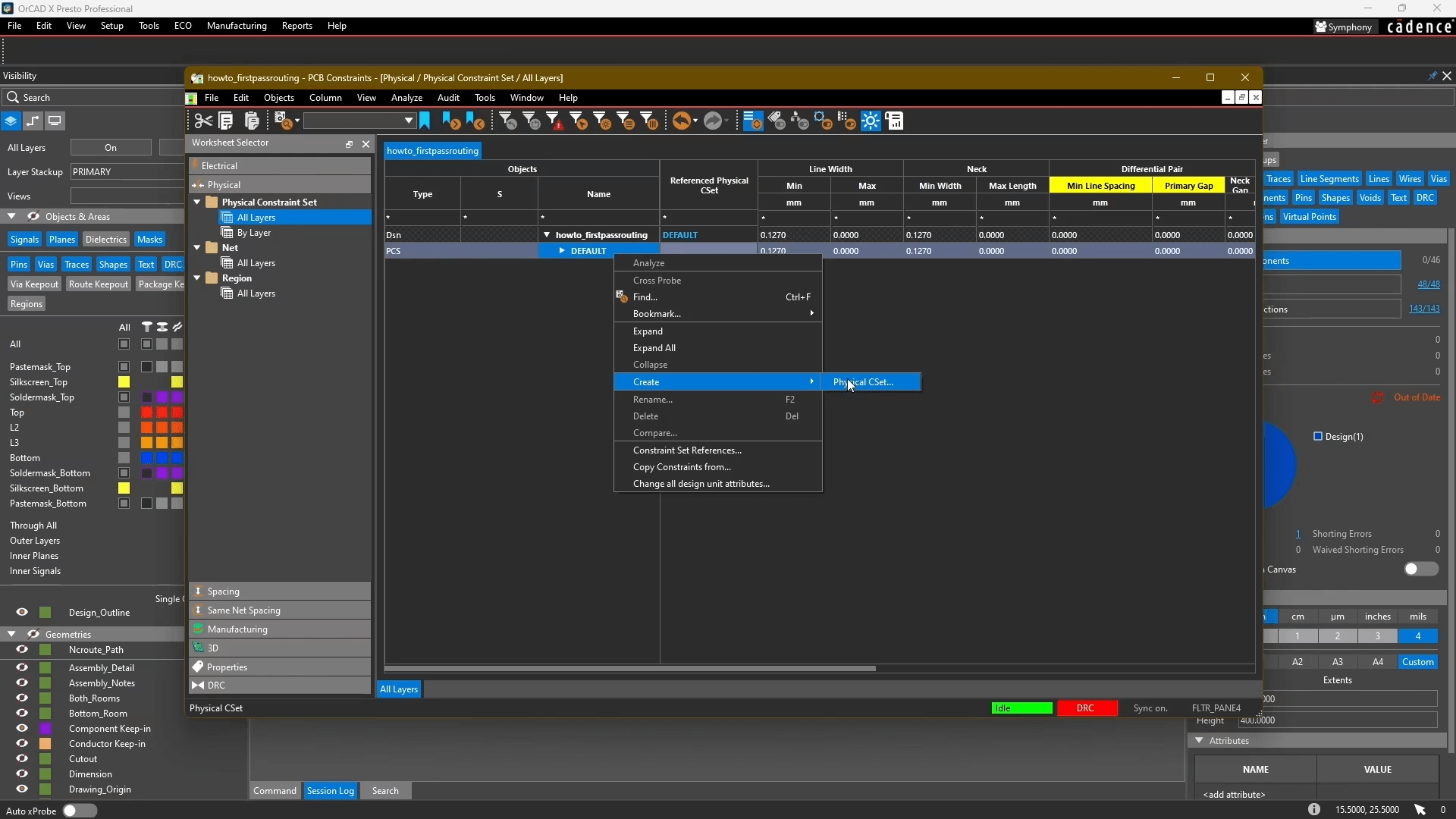
Through the constraint manager, CSETS are used to ensure different design parameters are adhered to. The image shows how to create a new CSET.
Setting Design Constraints in OrCAD X to Ensure Optimal PCB Design Parameters
Setting appropriate design constraints ensures that a PCB meets electrical, physical, and manufacturing requirements when designed in OrCAD X. The Constraint Manager allows users to edit constraint rules with the Constraint Manager, which allows designers to define trace widths, spacing via types, and differential pair settings.
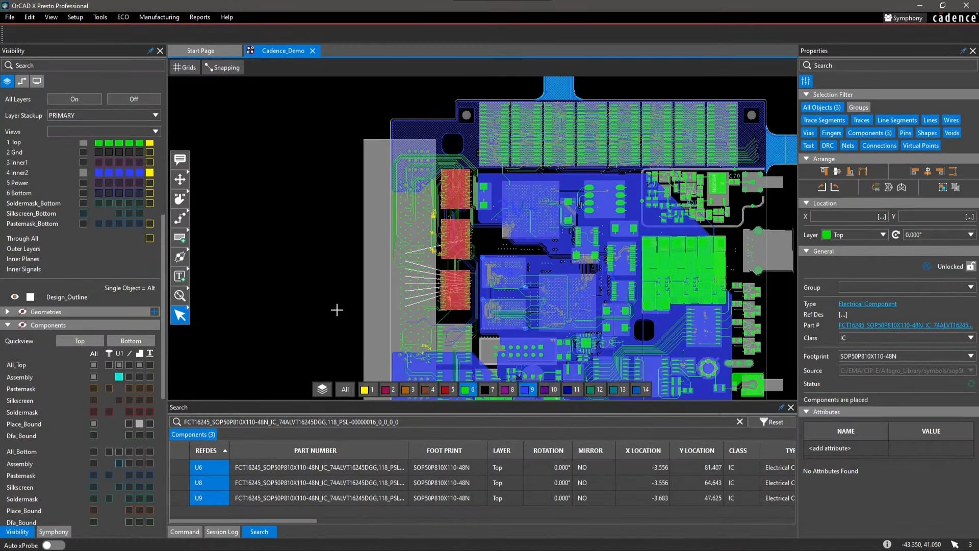
PCB Design Parameters in OrCAD X In The Constraint Manager
-
Open OrCAD X Layout.
-
Navigate to Tools > Constraint Manager.
-
The left panel contains different constraint categories, including Electrical, Physical, Spacing, and Manufacturing rules.
Defining Constraint Sets for Reusability
-
Constraint sets (CSet) act like templates that can be assigned to multiple nets or regions, reducing repetitive work.
-
To create a new constraint set:
-
Right-click Physical Constraint Set → Create Physical CSet.
-
Name the CSet appropriately (e.g., Power or Signal).
-
Assign values for minimum and maximum line width, neck width, and via types.
Setting Design Constraints for Key PCB Parameters
Electrical Constraints
Signal Integrity
-
Go to Electrical Constraints > Target Impedance, Propagation Delay.
-
Set trace width and spacing to control impedance.
-
Enable differential pair constraints for high-speed signals:
-
Select Electrical Constraint Set > Routing > Differential Pair.
-
Define maximum uncoupled length (e.g., 5.08 mm).
-
Set static phase tolerance (e.g., 0.508 mm).
-
Ensure EMI compliance by setting proper trace clearances.
Power Integrity
-
Define power plane constraints under Physical Constraint Sets.
-
Assign wider traces for power nets:
-
Minimum width: 0.508 mm (for power traces).
-
Maximum width: 2.54 mm (converted from 100 mils).
-
Apply decoupling capacitor rules for stable power distribution.
Physical Constraints
Board Dimensions
-
Ensure the PCB fits within the mechanical enclosure.
-
Set constraint rules for mounting hole placements.
Component Placement
-
Place high-speed components close to signal paths.
-
Assign power components near thermal reliefs.
-
Maintain proper spacing between analog and digital components to reduce interference.
Manufacturing Constraints
Design for Manufacturability (DFM)
-
Set trace width and spacing to meet fabrication requirements.
-
Use standard via sizes:
-
Assign Route Via type in Physical Constraint Manager.
-
Avoid unnecessary blind/buried vias unless required.
Material Selection
-
Choose high-frequency, low-loss materials for signal integrity.
-
Set up thermal constraints by enabling via stitching for heat dissipation.
Driving Design Choices by Constraints for an Optimized Final Product
Optimized Component Placement – Place high-speed components close to their corresponding signal paths to minimize interference; power components must have proper thermal dissipation areas.
Layer Stack-Up Decisions – The number and arrangement of PCB layers include constraints such as signal integrity, power distribution, and cost considerations. A well-planned stack-up reduces EMI and improves performance.
Manufacturability Considerations – Design-for-manufacturing (DFM) principles ensure the PCB is scalable while minimizing costs. Avoiding unnecessarily small features and aligning with manufacturer capabilities results in a smooth production process.
Ensuring PCB Design Parameters Are Met in OrCAD X
Verifying Design Rule Compliance
-
Run Analyze > Analysis Mode to check enabled rules.
-
Verify that constraints are applied correctly:
-
Yellow headers indicate rules that are OFF.
-
Right-click and select Analysis Mode to turn them ON.
-
Check real-time DRC errors in the Properties Panel.
-
Correct violations using slide adjustments in the PCB layout editor.
Ensuring Proper Routing Adherence
-
Use Add Connect Tool to route traces.
-
Flagged violations appear in white during routing.
-
Adjust trace paths to comply with spacing and impedance rules.
Reviewing and Fixing Errors
-
Open the DRC Summary Panel.
-
Click Pie Chart Segments to see categorized DRC violations.
-
Double-click an error to locate it on the PCB.
-
Modify the trace or component placement to fix the issue.
-
Run DRC refresh to validate corrections.
Optimizing PCB design parameters is essential for achieving high performance and manufacturability. Learn more about how OrCAD X can enhance your PCB design workflow and sign up for a free trial today.
Leading electronics providers rely on Cadence products to optimize power, space, and energy needs for a wide variety of market applications. To learn more about our innovative solutions, subscribe to our newsletter or our YouTube channel.