How to Plan for DDR Routing in PCB Layout
Key Takeaways
-
Setting up your design with the rules, constraints, footprints, and vias for DDR routing.
-
Considerations for routing DDR memory.
-
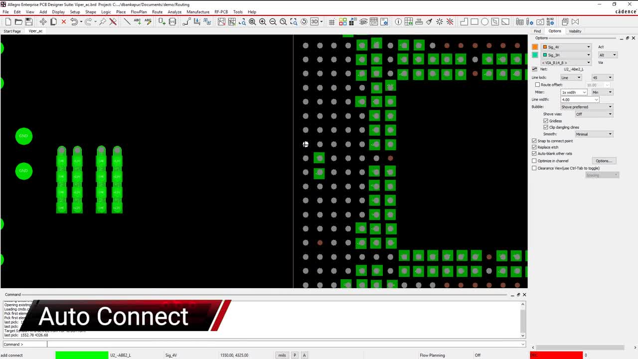
How your PCB design tools can help you with DDR memory routing.
DDR4 memory modules
For over 20 years now, DDR memory has been an integral part of PCB design. The initial DDR memory was soon superseded by DDR2, then DDR3, and finally by DDR4. With each new iteration of DDR memory, however, the PCB design challenges have become more complex. Pin counts have increased and the design constraints have become tighter, resulting in a whole lot of nets that need to be perfectly routed by the PCB designer.
The key to success in routing DDR memory is to be prepared for it before you start. This means planning your PCB design from the beginning for the type of routing that you need to do. Board materials, layer stackups, component placement, via types, and routing topologies all have to be planned for in advance. Here are some more details on how to plan for DDR routing in your next PCB design.
Setting Up Your Design for Successful DDR Memory Routing
The first step in preparing to design a board with DDR memory routing on it is to plan the board layers and configuration. Since you will be dealing with high-speed circuitry, you may need to consider other board materials than standard FR-4. But the most important part will be to configure your design layers for the board. Although you can squeeze dense routing into fewer layers, this will most likely not be the best configuration for signal integrity. You may be looking at 12 layers in your stackup for DDR routing due to the high density of the devices, and the need for stripline and dual stripline layer configurations.
The next step will be in setting up the rules and high-speed constraints for the design. A lot of the rules should already be included with the schematic data at the start of the design. You will most likely find more rules needed to load into the layout database, though. Here is where working with all members of the design team will pay off as you collect and organize the rules and constraints for the design. Since many of your designs may share similar traits and features, it is often helpful to maintain a library of design rules and constraints from previous designs to work with. This will help you to reduce the amount of time spent on this task.
As with any design, you will want to spend a good amount of time making sure that your PCB component footprints and land patterns are correct before you start. This will save you a lot of time later from having to correct and update parts that weren’t right in the first place. Not only will a mistake like this chip away at your schedule, but it could involve a massive amount of rework if an updated part no longer fits within the placement and routing that you’ve already completed.
You will also have to create new footprints for devices that you haven’t used before, such as the DDR memory parts. Here is where your online library resources can be a big help, such as the Unified Parts Search feature in the Cadence Allegro PCB design tools. For more information on working with PCB library symbols, take a look at the Rules for Schematic Symbols in this E-book.
Setting up the differential pairs in Allegro’s Constraint Manager
How to Plan for DDR Routing Using the Best Placement and Via Escapes
A good DDR routing plan requires that you first have good component placement. The same high-speed design methodologies that you’ve used before are still important here:
-
Signal paths: In high-speed design, you need to consider the entire signal path of sensitive circuits as opposed to only looking at point-to-point connections. This means working from the schematic to place the parts sequentially to keep the entire path from the driver to the receiver, and any parts in between, as close together as possible.
-
Memory devices: These parts need to be placed close together to minimize the routing between them and to keep them grouped. They should also be placed in order, starting with the lowest data bit and ending with the highest.
-
Routing channels: There will be a lot of nets to route with DDR memory and you need to intentionally place your parts for the expected routing room that you will need. Doing so will include enough room for the via escape patterns as well.
-
Sensitive circuitry: Give your sensitive high-speed circuitry enough room to isolate it from interference. This noise can come from other signals such as clocks, or power circuitry.
-
Bypass capacitors: To maintain the signal integrity in the memory circuitry, you will be placing a lot more bypass caps to stabilize the reference voltages. Make sure to give yourself enough room for these caps that won’t eat up the room already reserved for routing and escape vias.
You can find out additional details on placing components by reading this E-book on Steps for Successful Setup and Placement from Cadence. And speaking of escape vias, to successfully route DDR memory, you will need to have a good via escapement plan in place on your layout.
First, you will have to decide which vias to use; thru-hole, blind, or buried. You may even want to use micro vias to give yourself more space, but be aware of the costs increases for doing so. A lot of your via escapes will be from high pin-count ball grid array (BGA) parts. The smaller the pin pitch, the more you will want to use vias in the BGA pads. This will help you with routing out of the BGA patterns, but again there is a trade-off with manufacturing sophistication and cost. A very good resource here is to check with the vendor of the DDR components to find out their recommended vias escape routing patterns.
High-speed routing with tuned traces
DDR Memory Routing Considerations
Now you are ready to start planning the different routing strategies that are available to you for DDR memory routing. The topology of your routing will be determined by what group of signals you are working with. Daisy-chain routing is used for address and control routing, while point to point routing is used for sensitive circuits such as differential pairs. For DDR routing, however, there are some specific topologies to be aware of:
-
T-Topology: This is used for older DDR routing as it is unable to handle the higher signal rates that were introduced with DDR3 and DDR4. T-Topology will route the clocks, command, and address signals in a branch fashion from the controller to the memory devices while directly connecting the data lines.
-
Fly-by-termination: Fly-by routing differs from T-topology in that it routes the clocks, commands, and addresses in a chain from the controller to the different memory devices. The data lines still connect directly as they did in DDR2.
-
Clamshell: In this configuration, the memory devices are on the front and the back of the board. This results in less board space being used but complicates the routing. However, if successfully done, this strategy can help your routing by sharing vias between devices on the top and the bottom of the board.
Which topology you plan on will depend on what is needed for the circuitry and the layout of the board. Fly-by topologies are a big improvement over T-topologies in that they support higher-frequency operation as well as reducing the amount of routing, which improves signal integrity and timing. To read further on high-speed design issues such as noise and timing problems, take a look at this E-book from Cadence.
Because of the doubled data rate in DDR memory, it becomes very important to precisely route your trace lengths in order to meet the performance specifications of the device. With the ability to send and receive signals twice per clock cycle, the data must be captured on the rising and falling edge of its clock. To do this, the circuit timing must be precisely controlled, which is accomplished with controlling the trace lengths of the routing patterns. For other tips and tricks on PCB routing, check out this E-book on Your Route to Design Success.

Setting the Min/Max Propagation Delay on a Net Group from within the Constraint Manager
How Your Tools Can Help You Get to the Next Level
There’s a lot to plan for when you are preparing to design a circuit board with DDR routing in it. Another way that you can help yourself to be prepared for this level of design is using PCB design tools that have built-in advanced routing features and capabilities. You need to be able to easily set up your rules and design constraints as we’ve mentioned above, and having multiple features to help you route both manually and automatically is important. When routing DDR memory, it can also be helpful to separate the different memory groups by colors, and you will certainly need simulation and analysis tools built into your design system as well.
All of these features to help you with your DDR routing can be found in the best PCB design systems. The most advanced of these is Allegro PCB Designer from Cadence. With Allegro you will not only have the complete design system you need for today’s DDR routing considerations, but you will also be prepared for the next level of DDR memory routing and beyond.
If you’re looking to learn more about how Cadence has the solution for you, talk to us and our team of experts.