How Rapid Prototyping & Tooling Has Changed The Electronics Design Landscape
Key Takeaways
-
Learn how embedded system designers can leverage rapid prototyping boards.
-
Explore the potential of conductive-ink 3D printing.
-
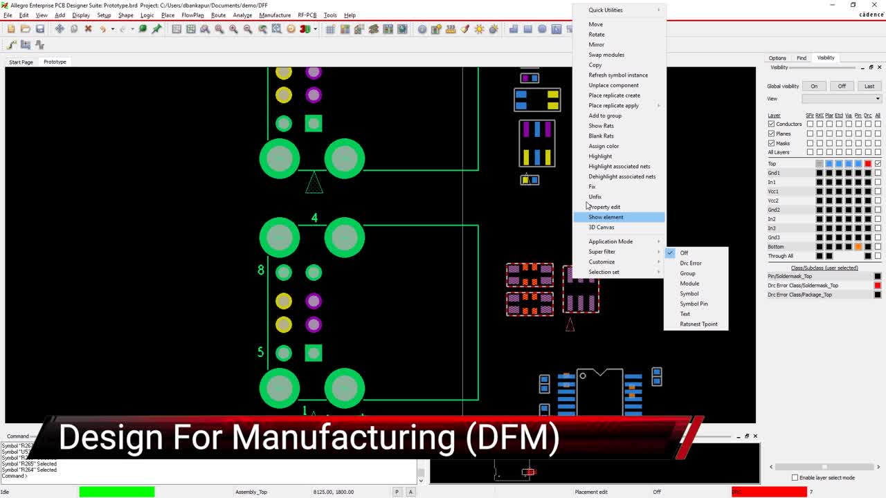
Understand how getting the right PCB software reduces design time.
Rapid prototyping boards enable engineers to start testing codes immediately.
How long does it take to make a perfect half-boiled egg? About 7 minutes. That’s what my experience of preparing breakfasts for years has taught me. A couple of minutes shorter will have the eggs turn up too raw and it’s overdone with a couple of minutes longer.
While I’ve yet to discover an unconventional means to shorten the time of making a half-boiled egg, the electronics industry has been making immense progress in reducing the design cycle of PCBs. New rapid prototyping and tooling technologies have been introduced to make the lives of electronics designers easier and more efficient
Rapid Prototyping Boards is Cutting Short Design Cycles
Embedded system designers have benefited greatly from the various rapid prototyping boards available. The old-school method of testing the viability of a project involves developing the hardware prototype from scratch. Time and resources are wasted on PCB design, manufacturing, and assembly just to get a few prototypes done.
Frustration can hit when design requirements are changed or if details are overlooked in the prototype. Today, embedded system designers are blessed with rapid prototyping boards like the Raspberry Pi, Arduino, BeagleBone, and Teensy. Microcontroller manufacturers have also joined the fray offering their versions of rapid prototyping kits.
These rapid prototyping boards have proven to be helpful as they allow minimal work in setting up the hardware. Often, the designer is then left to create a simpler I/O interface that connects to the board. With the prototyping duration reduced, the embedded system designer can quickly focus on running test codes on the hardware.
In some applications, these rapid prototyping boards continue to serve as the final hardware during deployment. For example, the Raspberry Pi, a powerful single-board computer that fits in the palm of your hand, has been deployed as a multimedia processor and an embedded temperature controller.
3D Printing Takes Rapid Prototyping & Tooling To The Next Level
3D printing allows the rapid manufacturing of PCB prototypes.
When 3D printers first hit the market, many were skeptical of their potential. Today, 3D printers have proven to be useful in almost any industry. The ability to turn CAD drawings into precisely crafted physical products is a dream for marketers.
3D printers have evolved beyond a tool for proof of concept into one that can manufacture high-quality industrial products. In electronics design, the introduction of conductive ink and filament has changed how low-volume PCBs are manufactured.
Instead of turning to large-scale PCB manufacturers, a 3D printer can be used to overlay a substrate with conductive inks or filaments. This process creates an accurate reproduction of the PCB layout that is fed to the 3D printing software. Some specialty 3D printers are even able to print multilayer circuits.
The innovation in 3D printing has been a handy time-saving measure. Not all PCB manufacturers are able to provide rapid prototyping services, and those that do may charge premium fees. If you’re constantly making revisions or executing new ideas, using a 3D printer can allow you to produce a new prototype in hours instead of days or weeks.
Advanced PCB Design Software Is Crucial In Reducing Design Time
Despite the emergence of 3D printing and rapid prototyping boards, PCB design remains a vital process in modern industry. Thankfully, much of the burden on designers is lifted by automation and the intelligence of built-in modern PCB software.
Getting the right software speeds up PCB design.
Gone are the days where PCB designers spent long hours creating footprints, arranging components, and routing traces between layers. Manufacturing files can now be generated with a couple of clicks. Not only that, the BOM list that links the components to manufacturers can also be created and managed within the right software.
You’ll be spared the guesswork in ensuring that the PCB is both functional and reliable. Design rule checks are easily configurable to weed out violations before the design is sent for fabrication. PCB design software has allowed designers to take a holistic approach, instead of dealing with a fragmented design cycle.
Today, designers increasingly rely on the advanced simulation and analysis tools offered by leading PCB design software. With a compatible layout tool like OrCAD PCB Designer, you’ll be certain to gain access to any verification process like crosstalk analysis or impedance management.
If you’re looking to learn more about how Cadence has the solution for you, talk to us and our team of experts.